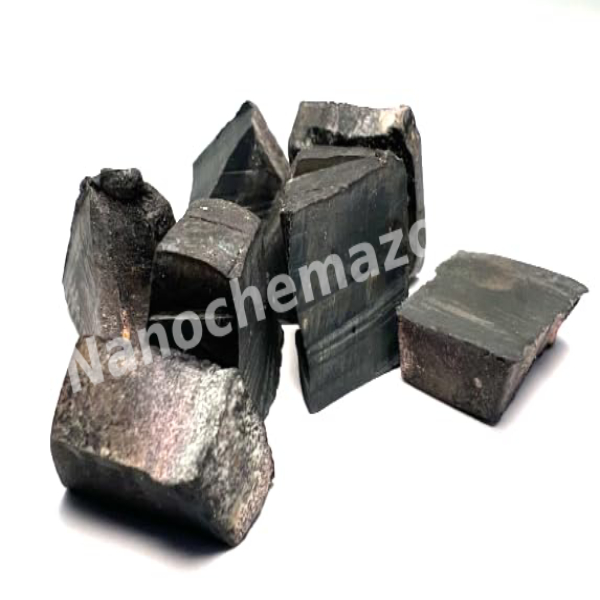
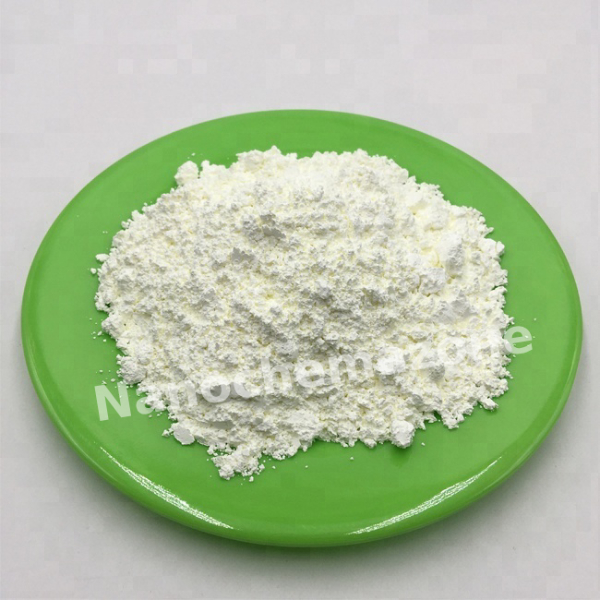
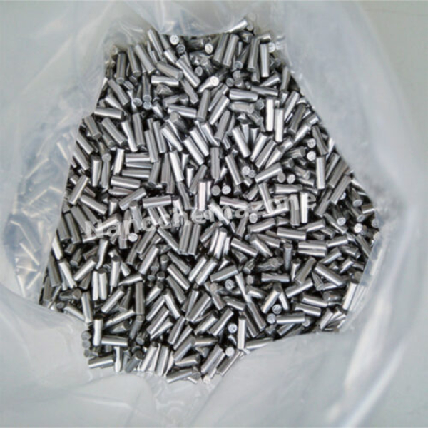
Iron-Nickel Nanoparticles, Fe65Ni35, APS: 50nm, Purity: 99.9%
Performance characteristics
Nano iron-nickel alloy powder is prepared by gas phase CVD method, the alloy ratio can be adjusted appropriately, the purity is high, the particle size is small, the distribution is uniform, the surface area is large, it is easy to disperse, and the industrial output is large. Low-frequency soft magnetic materials with high permeability and low coercivity in the magnetic field are commonly used in sensitive relays, magnetic shields, telephone and radio transformers, AC and DC meters, and current transformers (see transformers).
Applications
1. Nano-iron-nickel alloy powder has a wide range of application prospects in industries such as microwave absorbing materials, magnetic materials, hard alloys, and alloy coatings due to its special properties and special surface magnetism that are different from elemental iron and nickel metal powders;
2. Due to the refinement of nano-iron-nickel alloy grains, it is widely used in electronic products such as memory drums, magnetic cards, and magnetic tapes;
3. Powder metallurgy, auto parts, high specific gravity alloys, diamond tools, magnetic materials, electromagnetic shielding materials, which can be used as substitutes for pure metal nickel powder and cobalt powder;
4. The nano-iron-nickel alloy coating has a wide range of uses in protection, decoration, magnetism, etc. Its expansion coefficient is not much different from that of the nickel coating, so the peeling resistance is basically the same, but due to the addition of iron, the melting point of the iron-nickel alloy is high , And superior high-temperature strength and ductility, so the coating and molten steel have very good high-temperature resistance and thermal shock resistance, so it has excellent solderability and is very suitable for electronic components and printed circuit boards;
5. Nano-iron-nickel alloy can react with oxidizing corrosive gases, oxygen, chlorine, etc. to form a passivation film. It shows better corrosion resistance than iron in acid solutions and enhances the adhesion of the oxidized passivation layer. An anti-corrosion material.
Packaging and storage
This product is packaged in an inert gas glass bottle, sealed and stored in a dry, cool environment. It should not be exposed to the air to prevent oxidation and agglomeration due to moisture, which will affect the dispersion performance and use effect; the number of packages can be provided according to customer requirements and packed.