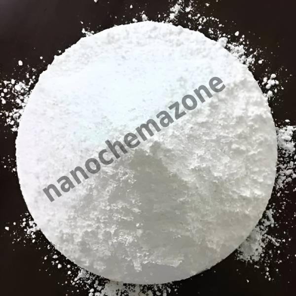
99.99% 4N 10 – 30 nm Gamma Aluminum Oxide (Alumina) Al2O3 Powder, 500 g

$319.00
Product 99.99% 4N 10 - 30 nm Gamma Aluminum Oxide (Alumina) Al2O3 Powder, 500 g
CAS No. 1344-28-1
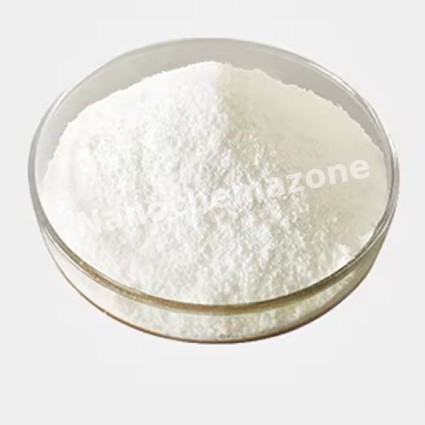
Appearance White to off-white
Purity ≥99%,  ≥99.9%,  ≥95%(Other purities are also available)
APS 10-30nm (Size Can be customized),  Ask for other available size range.
Ingredient Al2O3
Molecular Weight 101.96 g/mol
Melting Point N/A
Boiling Point N/A
Density 3.5–3.7 g/cm³
Product Codes NCZ-237I
 

99.99% 4N 10-20 nm Aluminum Oxide (Alumina) Al2O3 Powder, 500 g

$319.00
Product 99.99% 4N 10-20 nm Aluminum Oxide (Alumina) Al2O3 Powder, 500 g
CAS No. 1344-28-1
Appearance White to off-white
Purity ≥99%,  ≥99.9%,  ≥95%(Other purities are also available)
APS 10-20nm (Size Can be customized),  Ask for other available size range.
Ingredient Al2O3
Molecular Weight 101.96 g/mol
Melting Point N/A
Boiling Point N/A
Density 3.6–3.7 g/cm³
Product Codes NCZ-238I

Chlorine Functionalized Graphene Quantum Dots Solution, 1mg/mL

Price range: $319.00 through $555.00
Select options This product has multiple variants. The options may be chosen on the product page
Product Chlorine Functionalized Graphene Quantum Dots Solution, 1mg/mL
CAS No. N/A
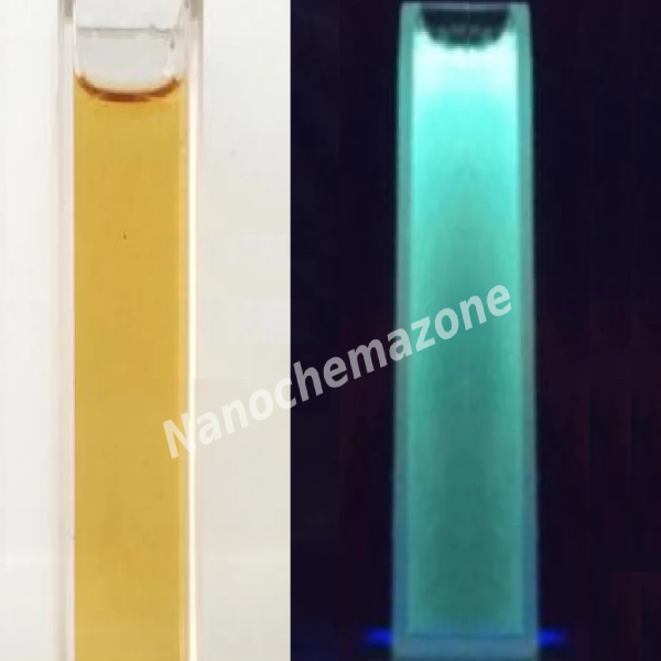
Appearance Clear yellowish aqueous
Purity ≥99%,  ≥99.9%,  ≥95%(Other purities are also available)
APS 4–12nm (Size Can be customized),  Ask for other available size range.
Ingredient CₓHᵧO_zCl_w
Molecular Weight N/A
Melting Point N/A
Boiling Point N/A
Density N/A
Product Codes NCZ-317I

Lithium Titanate (Li2TiO3) Sputtering Targets, indium, Purity: 99.95%, Size: 2”, Thickness: 0.125”

$319.00

Product 

Lithium Titanate (Li2TiO3) Sputtering Targets, indium, Purity: 99.95%, Size: 2'', Thickness: 0.125''

CAS No.

12031-82-2

Appearance

Powder

Purity

≥99%,  ≥99.9%,  ≥95%

(Other purities are also available)

APS

 N/A (Size Can be customized), Ask for other available size ranges.

Ingredient

N/A

Molecular Weight

109.75 g/mol

Melting Point

Decomposes before melting (~1,200 °C)

Boiling Point

N/A

Density

~3.41 g/cm³

Product Codes

NCZ-2009K

High Purity Lead (II) Iodide (PbI2) Trace Metals Basis, Perovskite Grade, 99.999%, 5N, 10g

$319.00
Product High Purity Lead (II) Iodide (PbI2) Trace Metals Basis, Perovskite Grade, 99.999%, 5N, 10g
CAS No. 10101-63-0
Appearance Bright yellow to orange crystalline
Purity ≥99%,  ≥99.9%,  ≥95%(Other purities are also available)
APS N/A
Ingredient PbI2
Molecular Weight 461.01 g/mol
Melting Point N/A
Boiling Point N/A
Density 6.16 g/cm³
Product Codes NCZ-410I
 

Hydroxy Graphene Quantum Dots Solution, 1mg/mL

Price range: $319.00 through $480.00
Select options This product has multiple variants. The options may be chosen on the product page
Product Hydroxy Graphene Quantum Dots Solution, 1mg/mL
CAS No. N/A
Appearance Clear to light yellow or brown
Purity ≥99%,  ≥99.9%,  ≥95%(Other purities are also available)
APS 10nm (Size Can be customized),  Ask for other available size range.
Ingredient CₓHᵧO_z
Molecular Weight N/A
Melting Point N/A
Boiling Point N/A
Density N/A
Product Codes NCZ-421I

Silicon Disulfide, SiS2, 99.999% 5N High Purity Powder

Price range: $319.00 through $825.00
Select options This product has multiple variants. The options may be chosen on the product page
Product Silicon Disulfide, SiS2, 99.999% 5N High Purity Powder
CAS No. 13514-63-3
Appearance White to pale yellow
Purity ≥99%,  ≥99.9%,  ≥95%(Other purities are also available)
APS 10µm (Size Can be customized),  Ask for other available size range.
Ingredient SiS2
Molecular Weight 90.19 g/mol
Melting Point N/A
Boiling Point N/A
Density N/A
Product Codes NCZ-518I
 

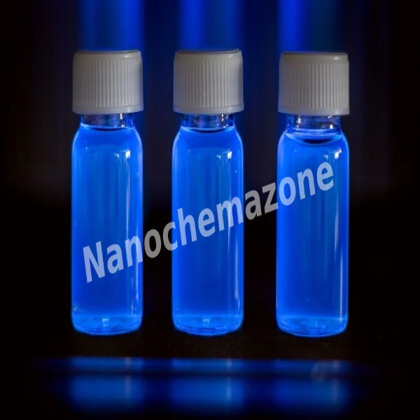
Silicon Quantum Dots Solution (Blue Fluorescence)

$319.00
Select options This product has multiple variants. The options may be chosen on the product page
Product Silicon Quantum Dots Solution (Blue Fluorescence)
CAS No. N/A
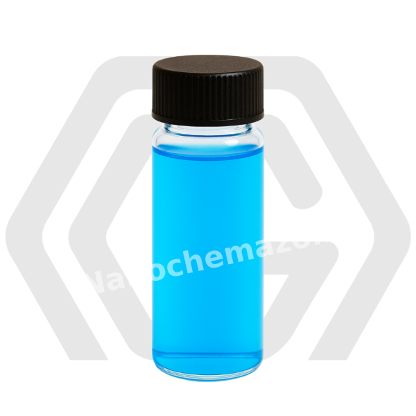
Appearance Clear to slightly colored colloidal
Purity ≥99%,  ≥99.9%,  ≥95%(Other purities are also available)
APS 2–4nm (Size Can be customized),  Ask for other available size range.
Ingredient Si
Molecular Weight N/A
Melting Point N/A
Boiling Point N/A
Density 2.33 g/cm³
Product Codes NCZ-520I
 

Titanate Nanotubes Powder, 1g/bottle

$319.00
Product Titanate Nanotubes Powder, 1g/bottle
CAS No. 12031-82-2
Appearance Fine, white/off-white
Purity ≥99%,  ≥99.9%,  ≥95%(Other purities are also available)
APS 10–20nm (Size Can be customized),  Ask for other available size range.
Ingredient H₂Ti₃O₇
Molecular Weight 242.52 g/mol
Melting Point N/A
Boiling Point N/A
Density 3.12–3.16 g/cm³
Product Codes NCZ-567I

Tungsten Titanium (TiW) Sputtering Targets, Purity: 99.99%, Size: 2”, Thickness: 0.250”

$320.00

Applications of Sputtering Targets;

Film deposition is accomplished using sputtering targets. A technique for sputtering thin films is called "deposition made by sputter targets," which entails eroding material from a "target" source onto a "substrate" like a silicon wafer. Etching of the target is done using semiconductor sputtering targets. When selectivity is not an issue and a high degree of etching anisotropy is required, sputter etching is the method of choice. By removing the target material through etching, sputter targets are also utilized for investigation. In secondary ion spectroscopy (SIMS), one example is when the target material is sputtered at a steady pace. Mass spectrometry is used to quantify the concentration and identity of spewed atoms as the target is sputtered.

The target material's composition may be ascertained and even very low concentrations of contaminants can be found with the aid of the sputtering target.

There is also an application area for sputtering targets in space. One type of space weathering that alters the chemical and physical characteristics of airless worlds like the Moon and asteroids is sputtering.

High Purity Atomized Spherical Magnesium (Mg) Powder NGW120

Price range: $321.00 through $1,668.00
Select options This product has multiple variants. The options may be chosen on the product page
500 grams/285 € 1 kg/390 € 5 kg/1480 €  
Please contact us for quotes on larger quantities !!!

High Purity Atomized Spherical Magnesium (Mg) Powder NGW120

High purity atomized spherical magnesium powder is manufacturing by the centrifugal atomization technology that is melting minimum 99.8% purity magnesium and spraying the molten metal under the protection of an inert atmosphere. High purity atomized spherical magnesium powder is known with the outstanding features of high apparent density, high content of active magnesium, high fluidity, high stability, small particle size and small specific surface, and so on.

Technical Properties:

Particle Shape

Spherical Particle

Spherical Rate (%)

≥95

Apparent Density (g·cm-3 )

0.9 (min)

Bulk Density (g·cm-3 )

0.97 (min)

Liquidity (s·(50g)-1 )

78.6

Moisture Absorption (%)

0.01

Active Mg Content (%)

99.0 (min)

Impurity Content (%)

Moisture Content (%max)

0.08

HCl Undissolved Substance (%max)

0.047

Oil content (%max)

0.00

Fe (%max)

0.045

Mn (%max)

0.008

Zn (%max)

0.008

Cl (%max)

0.004


Particle Size Distribution:

Particle Distributing

D50 (µm)

Granularity/µm

Percentage (%) Not more than

≥600

0

120±10

≥300

10.0

≥150

40.0

<75

30.0

<45

5.0


Applications:

High purity atomized spherical magnesium powder is widely used in the fields like aviation, national defense, composite materials, powder metallurgy, petrochemical catalyst, electronic coating, medicine, foods and new type functional materials and so on.

Praseodymium (Pr) Sputtering Targets, Purity: 99.9%, Size: 4”, Thickness: 0.250”

$322.00

Applications of Sputtering Targets;

  • Sputtering targets is used for film deposition. The deposition made by sputter targets is a method of depositing thin films by sputtering that involves eroding material from a "target" source onto a "substrate" such as  a silicon wafer.
  • Semiconductor sputtering targets is used to etch the target. Sputter etching is chosen in cases where a high degree of etching anisotropy is needed and selectivity is not a concern.
  • Sputter targets is also used for analysis by etching away the target material.
One of the example occurs in secondary ion spectroscopy (SIMS), where the target sample is sputtered at a constant rate. As the target is sputtered, the concentration and identity of sputtered atoms are measured using mass spectrometry. By helping of the sputtering target, the composition of the target material can be determined and even extremely low concentrations of impurities are detected. Sputtering target has also application area in space. Sputtering is one of the forms of space weathering, a process that changes the physical and chemical properties of airless bodies, such as asteroids and the Moon.

Nickel (Ni) Sputtering Targets, Purity: 99.995%, Size: 4”, Thickness: 0.250”

$322.00

Applications of Sputtering Targets;

Film deposition is accomplished using sputtering targets. A technique for sputtering thin films is called "deposition made by sputter targets," which entails eroding material from a "target" source onto a "substrate" like a silicon wafer. Etching of the target is done using semiconductor sputtering targets. When selectivity is not an issue and a high degree of etching anisotropy is required, sputter etching is the method of choice. By removing the target material through etching, sputter targets are also utilized for investigation. In secondary ion spectroscopy (SIMS), one example is when the target material is sputtered at a steady pace. Mass spectrometry is used to quantify the concentration and identity of spewed atoms as the target is sputtered.

By helping of the sputtering target, the composition of the target material may be evaluated and even extremely tiny amounts of contaminants are recognized.

There is also an application area for sputtering targets in space. One type of space weathering that alters the chemical and physical characteristics of airless worlds like the Moon and asteroids is sputtering.

Praseodymium (Pr) Sputtering Targets, Purity: 99.9%, Size: 4”, Thickness: 0.250”

$322.00

Applications of Sputtering Targets;

Film deposition is accomplished using sputtering targets. A technique for sputtering thin films is called "deposition made by sputter targets," which entails eroding material from a "target" source onto a "substrate" like a silicon wafer. Etching of the target is done using semiconductor sputtering targets. When selectivity is not an issue and a high degree of etching anisotropy is required, sputter etching is the method of choice. By removing the target material through etching, sputter targets are also utilized for investigation. In secondary ion spectroscopy (SIMS), one example is when the target material is sputtered at a steady pace. Mass spectrometry is used to quantify the concentration and identity of spewed atoms as the target is sputtered.

The target material's composition may be ascertained and even very low concentrations of contaminants can be found with the aid of the sputtering target.

There is also an application area for sputtering targets in space. One type of space weathering that alters the chemical and physical characteristics of airless worlds like the Moon and asteroids is sputtering.

Vanadium (V) Sputtering Targets, Purity: 99.5%, Size: 2”, Thickness: 0.250”

$323.00

Product 

Vanadium (V) Sputtering Targets, Purity: 99.5%, Size: 2'', Thickness: 0.250''

CAS No.

7440-62-2

Appearance

Powder

Purity

≥99%,  ≥99.9%,  ≥95%

(Other purities are also available)

APS

N/A  (Size Can be customized), Ask for other available size ranges.

Ingredient

N/A

Molecular Weight

50.9415 g/mol

Melting Point

1910 °C

Boiling Point

3407 °C

Density

6.11 g/cm³

Product Codes

NCZ-1549K

Molybdenum (Mo) Sputtering Targets, Purity: 99.95%, Size: 8”, Thickness: 0.250”

$323.00

Product 

Molybdenum (Mo) Sputtering Targets, Purity: 99.95%, Size: 8'', Thickness: 0.250''

CAS No.

 7439-98-7

Appearance

Powder

Purity

≥99%,  ≥99.9%,  ≥95%

(Other purities are also available)

APS

 N/A (Size Can be customized), Ask for other available size ranges.

Ingredient

N/A

Molecular Weight

95.95 g/mol

Melting Point

 2623 °C

Boiling Point

 4639 °C

Density

10.28 g/cm³

Product Codes

NCZ-1930K

Monolayer Graphene on SiO2/Si Substrate, Size: 3″

Price range: $324.00 through $1,369.00
Select options This product has multiple variants. The options may be chosen on the product page

Applications

Graphene research; Supercapacitors; Catalyst; Solar energy; Graphene optoelectronics, plasmonics and nanophotonics; Graphene semiconductor chips; Conductive graphene film; Graphene computer memory; Biomaterials and Bioelectronics.

Magnesium Fluoride (MgF2) Sputtering Targets, Purity: 99.9%, Size: 3”, Thickness: 0.250”

$324.00

Applications of Sputtering Targets;

Film deposition is accomplished using sputtering targets. A technique for sputtering thin films is called "deposition made by sputter targets," which entails eroding material from a "target" source onto a "substrate" like a silicon wafer. Etching of the target is done using semiconductor sputtering targets. When selectivity is not an issue and a high degree of etching anisotropy is required, sputter etching is the method of choice. By removing the target material through etching, sputter targets are also utilized for investigation. In secondary ion spectroscopy (SIMS), one example is when the target material is sputtered at a steady pace. Mass spectrometry is used to quantify the concentration and identity of spewed atoms as the target is sputtered.

The target material's composition may be ascertained and even very low concentrations of contaminants can be found with the aid of the sputtering target.

There is also an application area for sputtering targets in space. One type of space weathering that alters the chemical and physical characteristics of airless worlds like the Moon and asteroids is sputtering.

Titanium Boride (TiB2) Sputtering Targets, Purity: 99.5%, Size: 1”, Thickness: 0.250”

$324.00

Applications of Sputtering Targets;

Film deposition is accomplished using sputtering targets. A technique for sputtering thin films is called "deposition made by sputter targets," which entails eroding material from a "target" source onto a "substrate" like a silicon wafer. Etching of the target is done using semiconductor sputtering targets. When selectivity is not an issue and a high degree of etching anisotropy is required, sputter etching is the method of choice. By removing the target material through etching, sputter targets are also utilized for investigation. In secondary ion spectroscopy (SIMS), one example is when the target material is sputtered at a steady pace. Mass spectrometry is used to quantify the concentration and identity of spewed atoms as the target is sputtered.

The target material's composition may be ascertained and even very low concentrations of contaminants can be found with the aid of the sputtering target.

There is also an application area for sputtering targets in space. One type of space weathering that alters the chemical and physical characteristics of airless worlds like the Moon and asteroids is sputtering.

Titanium Dioxide (TiO2) Sputtering Targets, Purity: 99.9%, Size: 1”, Thickness: 0.250”, Grey to Black

$324.00

Product 

Titanium Dioxide (TiO2) Sputtering Targets, Purity: 99.9%, Size: 1'', Thickness: 0.250'', Grey to Black

CAS No.

13463‑67‑7

Appearance

Powder

Purity

≥99%,  ≥99.9%,  ≥95%

(Other purities are also available)

APS

TiO₂ (black granules) (Size Can be customized), Ask for other available size ranges.

Ingredient

N/A

Molecular Weight

79.94 g/mol

Melting Point

~1,843 °C

Boiling Point

~2,972 °C

Density

~4.23 g/cm³

Product Codes

NCZ-1443K

Silicon Nitride (Si3N4) Sputtering Targets, Purity: 99.9%, Size: 1”, Thickness: 0.250”, White to Gray

$324.00

Product 

Silicon Nitride (Si3N4) Sputtering Targets, Purity: 99.9%, Size: 1'', Thickness: 0.250'', White to Gray

CAS No.

 12033-89-5

Appearance

Powder

Purity

≥99%,  ≥99.9%,  ≥95%

(Other purities are also available)

APS

N/A  (Size Can be customized), Ask for other available size ranges.

Ingredient

N/A

Molecular Weight

 140.28 g/mol

Melting Point

 ~1900 °C

Boiling Point

N/A

Density

~3.2 g/cm³

Product Codes

NCZ-1702K

Molybdenum (Mo) Sputtering Targets, Purity: 99.95%, Size: 6”, Thickness: 0.250”

$325.00

Applications of Sputtering Targets;

Film deposition is accomplished using sputtering targets. A technique for sputtering thin films is called "deposition made by sputter targets," which entails eroding material from a "target" source onto a "substrate" like a silicon wafer. Etching of the target is done using semiconductor sputtering targets. When selectivity is not an issue and a high degree of etching anisotropy is required, sputter etching is the method of choice. By removing the target material through etching, sputter targets are also utilized for investigation. In secondary ion spectroscopy (SIMS), one example is when the target material is sputtered at a steady pace. Mass spectrometry is used to quantify the concentration and identity of spewed atoms as the target is sputtered.

By helping of the sputtering target, the composition of the target material may be evaluated and even extremely tiny amounts of contaminants are recognized.

There is also an application area for sputtering targets in space. One type of space weathering that alters the chemical and physical characteristics of airless worlds like the Moon and asteroids is sputtering.

α-Tricalcium phosphate(α-Ca3(PO4)2, >95%) (207982)

$325.00
Select options This product has multiple variants. The options may be chosen on the product page

Product 

α-Tricalcium phosphate(α-Ca3(PO4)2, >95%) (207982)

CAS No.

7758‑87‑4

Appearance

Powder

Purity

≥99%,  ≥99.9%,  ≥95%

(Other purities are also available)

APS

  <80um (Size Can be customized), Ask for other available size ranges.

Ingredient

N/A

Molecular Weight

~310.18 g/mol

Melting Point

~1670 °C

Boiling Point

N/A

Density

~2.866 g/cm³

Product Codes

NCZ-2610K

Alginate Oligosaccharide(Food grade) (233589)

$325.00
Select options This product has multiple variants. The options may be chosen on the product page
Alginate Oligosaccharide(Food grade) (233589)

Alginate oligosaccharide, produced by the degradation of algin, is a linear polysaccharide consisting of α-L-guluronate (G) and β-D-mannuronate (M) is the latest generation of functional oligosaccharides.

Specifications:

Test Items Specifications
Appearance Off white Powder
Content (%) ≥85
Particle size (Mesh) ≥100
Moisture(%) ≤10.0
Ash Content(%) ≤1.0
Insoluble(%) ≤0.6
pH value 4.5-7.0
Pb(ppm) ≤1.0
As(ppm) ≤0.5
Mercury(ppm) ≤0.5
Total plate count(cfu/g) ≤1000
Yeast and Mold(cfu/g) ≤30
Pathogen(cfu/g) Negative
Product Codes- NCZ-2660K

Ectoin (539511)

$325.00
Select options This product has multiple variants. The options may be chosen on the product page
Ectoin (539511) Description: Ectoin is a cyclic amino acid derivative obtained through fermentation technology. As an important substance for microorganism to survive in extreme environments, ectoin can effectively bind the surrounding water molecules and form a protective layer on the surface of cell membrane, to fully protect intracellular substance from UV light and high temperature, etc. Ectoin has remarkable moisturizing, soothing and repairing effects, and is widely used in various cosmetic formulations. INCI Name: Ectoin CAS No.: 96702-03-3 Structural formula: . . . . . Applications: essence, lotion, face cream, facial mask, cosmetic water, etc. User guide: adding at low temperature after emulsification Recommended dosage: 0.1%-5% Shelf life: 24 months Storage: stored in sealed and cool condition, at room temperature Physical and chemical properties 
Items Standard
Appearance White or off-white powder or granules
Assay ≥ 98%.
pH 5.0~7.5
Transmittance ≥ 98%
Specific rotation +139° ~ +145°
Chlorine ≤ 0.05%
Loss on drying ≤ 1.0%
Ignition residue ≤ 1.0%
Heavy metals ≤ 10.0 ppm
Pb ≤ 2.0 ppm
Total Plate Count ≤ 100 cfu/g
Molds and yeasts count ≤ 50 cfu/g
Thermophilic coliform Negative
Pseudomonas Aeruginosa Negative
Staphylococcus aureus Negative
Product Codes- NCZ-2716K

Copper (Cu) Sputtering Targets, Purity: 99.999%, Size: 4”, Thickness: 0.125”

$326.00

Product 

Copper (Cu) Sputtering Targets, Purity: 99.999%, Size: 4'', Thickness: 0.125''

CAS No.

7440-50-8

Appearance

Powder

Purity

≥99%,  ≥99.9%,  ≥95%

(Other purities are also available)

APS

 N/A (Size Can be customized), Ask for other available size ranges.

Ingredient

N/A

Molecular Weight

63.55 g/mol

Melting Point

1,084 °C

Boiling Point

 2,562 °C

Density

8.96 g/cm³

Product Codes

NCZ-2261K

Calcium Manganate (CaMnO3) Sputtering Targets, Purity: 99.9%, Size: 1”, Thickness: 0.125”

$326.00

Product 

Calcium Manganate (CaMnO3) Sputtering Targets, Purity: 99.9%, Size: 1'', Thickness: 0.125''

CAS No.

12058-85-6

Appearance

Powder

Purity

≥99%,  ≥99.9%,  ≥95%

(Other purities are also available)

APS

 N/A (Size Can be customized), Ask for other available size ranges.

Ingredient

N/A

Molecular Weight

157.87 g/mol

Melting Point

 Approx. 1400 °C (decomposes)

Boiling Point

N/A

Density

 ~4.7 g/cm³

Product Codes

NCZ-2363K

Selenium (Se) Sputtering Targets, Purity: 99.999%, Size: 3”, Thickness: 0.250”

$327.00

Applications of Sputtering Targets;

Film deposition is accomplished using sputtering targets. A technique for sputtering thin films is called "deposition made by sputter targets," which entails eroding material from a "target" source onto a "substrate" like a silicon wafer. Etching of the target is done using semiconductor sputtering targets. When selectivity is not an issue and a high degree of etching anisotropy is required, sputter etching is the method of choice. By removing the target material through etching, sputter targets are also utilized for investigation. In secondary ion spectroscopy (SIMS), one example is when the target material is sputtered at a steady pace. Mass spectrometry is used to quantify the concentration and identity of spewed atoms as the target is sputtered.

Vanadium Oxide (V2O5) Sputtering Targets, Purity: 99.9%, Size: 2”, Thickness: 0.125”

$327.00

Applications of Sputtering Targets;

Film deposition is accomplished using sputtering targets. A technique for sputtering thin films is called "deposition made by sputter targets," which entails eroding material from a "target" source onto a "substrate" like a silicon wafer. Etching of the target is done using semiconductor sputtering targets. When selectivity is not an issue and a high degree of etching anisotropy is required, sputter etching is the method of choice. By removing the target material through etching, sputter targets are also utilized for investigation. In secondary ion spectroscopy (SIMS), one example is when the target material is sputtered at a steady pace. Mass spectrometry is used to quantify the concentration and identity of spewed atoms as the target is sputtered.

The target material's composition may be ascertained and even very low concentrations of contaminants can be found with the aid of the sputtering target.

There is also an application area for sputtering targets in space. One type of space weathering that alters the chemical and physical characteristics of airless worlds like the Moon and asteroids is sputtering.

Zinc Oxide (ZnO) Sputtering Targets, Purity: 99.9%, Size: 1”, Thickness: 0.125”

$327.00

Applications of Sputtering Targets;

Film deposition is accomplished using sputtering targets. A technique for sputtering thin films is called "deposition made by sputter targets," which entails eroding material from a "target" source onto a "substrate" like a silicon wafer. Etching of the target is done using semiconductor sputtering targets. When selectivity is not an issue and a high degree of etching anisotropy is required, sputter etching is the method of choice. By removing the target material through etching, sputter targets are also utilized for investigation. In secondary ion spectroscopy (SIMS), one example is when the target material is sputtered at a steady pace. Mass spectrometry is used to quantify the concentration and identity of spewed atoms as the target is sputtered.

The target material's composition may be ascertained and even very low concentrations of contaminants can be found with the aid of the sputtering target.

There is also an application area for sputtering targets in space. One type of space weathering that alters the chemical and physical characteristics of airless worlds like the Moon and asteroids is sputtering.

Carbon Nanotube Sponges, Size: 20 mm x 20 mm, Thickness: 1-2 mm

Price range: $328.00 through $1,573.00
Select options This product has multiple variants. The options may be chosen on the product page
Carbon Nanotube Sponges, Size: 20 mm x 20 mm, Thickness: 1-2mm The carbon nanotube sponge structure is uniform and they possess good mechanical strength, good flexibility, high porosity and low density. They can be used as a purifying agent in order to absorb pollutants. These pollutants can be fertilizers, pesticides or pharmaceuticals found in water, energy storage materials, catalyst carriers or in high-efficiency composite materials.

Boron (B) Sputtering Targets, Purity: 99.9%, Size: 2”, Thickness: 0.250”

$328.00

Applications of Sputtering Targets;

Film deposition is accomplished using sputtering targets. A technique for sputtering thin films is called "deposition made by sputter targets," which entails eroding material from a "target" source onto a "substrate" like a silicon wafer. Etching of the target is done using semiconductor sputtering targets. When selectivity is not an issue and a high degree of etching anisotropy is required, sputter etching is the method of choice. By removing the target material through etching, sputter targets are also utilized for investigation. In secondary ion spectroscopy (SIMS), one example is when the target material is sputtered at a steady pace. Mass spectrometry is used to quantify the concentration and identity of spewed atoms as the target is sputtered.

The target material's composition may be ascertained and even very low concentrations of contaminants can be found with the aid of the sputtering target.

There is also an application area for sputtering targets in space. One type of space weathering that alters the chemical and physical characteristics of airless worlds like the Moon and asteroids is sputtering.

Ytterbium (Yb) Sputtering Target

Price range: $328.00 through $1,520.00
Select options This product has multiple variants. The options may be chosen on the product page

Product 

Ytterbium (Yb) Sputtering Target

CAS No.

7440‑64‑4

Appearance

Powder

Purity

≥99%,  ≥99.9%,  ≥95%

(Other purities are also available)

APS

 NA (Size Can be customized), Ask for other available size ranges.

Ingredient

N/A

Molecular Weight

50.9415 g/mol

Melting Point

~824 °C

Boiling Point

~1,196 °C

Density

~6.9 g/cm³

Product Codes

NCZ-1309K

Nickel (Ni) Sputtering Targets, Purity: 99.99%, Size: 5”, Thickness: 0.250”

$328.00

Product 

Nickel (Ni) Sputtering Targets, Purity: 99.99%, Size: 5'', Thickness: 0.250''

CAS No.

7440-02-0

Appearance

Powder

Purity

≥99%,  ≥99.9%,  ≥95%

(Other purities are also available)

APS

 N/A (Size Can be customized), Ask for other available size ranges.

Ingredient

N/A

Molecular Weight

 58.69 g/mol

Melting Point

 1,455 °C

Boiling Point

 2,732 °C

Density

 8.90 g/cm³

Product Codes

NCZ-1874K

Lead (Pb) Sputtering Targets, Purity: 99.99+%, Size: 3”, Thickness: 0.125”

$328.00

Product 

Lead (Pb) Sputtering Targets, Purity: 99.99+%, Size: 3'', Thickness: 0.125''

CAS No.

7439‑92‑1

Appearance

Powder

Purity

≥99%,  ≥99.9%,  ≥95%

(Other purities are also available)

APS

 N/A (Size Can be customized), Ask for other available size ranges.

Ingredient

N/A

Molecular Weight

 207.2 g/mol

Melting Point

~327.5 °C

Boiling Point

~1,740 °C

Density

 ~11.34 g/cm³

Product Codes

NCZ-2074K

Selenium Sputtering Target Se

Price range: $329.00 through $759.00
Select options This product has multiple variants. The options may be chosen on the product page
Product Selenium Sputtering Target Se
CAS No. 7782-49-2
Appearance Gray, Metallic Luster, Non-Metallic
Purity ≥99%,  ≥99.9%,  ≥95%(Other purities are also available)
APS 1–10 µm (Size Can be customized),  Ask for other available size range.
Ingredient Se
Molecular Weight 78.96 g/mol
Melting Point N/A
Boiling Point N/A
Density 4.79 g/cm
Product Codes NCZ-135H
 

Bismuth (Bi) Sputtering Targets, Purity: 99.999%, Size: 3”, Thickness: 0.250”

$329.00

Product 

Bismuth (Bi) Sputtering Targets, Purity: 99.999%, Size: 3'', Thickness: 0.250''

CAS No.

7440‑69‑9

Appearance

Powder

Purity

≥99%,  ≥99.9%,  ≥95%

(Other purities are also available)

APS

1 – 5 µm (Size Can be customized), Ask for other available size ranges.

Ingredient

N/A

Molecular Weight

~208.98 g/mol

Melting Point

 271.4 °C

Boiling Point

~1560 °C

Density

 ~9.78–9.80 g/cm³

Product Codes

NCZ-2435K

Bismuth (Bi) Sputtering Targets, Purity: 99.999%, Size: 4”, Thickness: 0.125”

$330.00

Applications of Sputtering Targets;

Film deposition is accomplished using sputtering targets. A technique for sputtering thin films is called "deposition made by sputter targets," which entails eroding material from a "target" source onto a "substrate" like a silicon wafer.

Etching of the target is done using semiconductor sputtering targets. When selectivity is not an issue and a high degree of etching anisotropy is required, sputter etching is the method of choice. By removing the target material through etching, sputter targets are also utilized for investigation. In secondary ion spectroscopy (SIMS), one example is when the target material is sputtered at a steady pace. Mass spectrometry is used to quantify the concentration and identity of spewed atoms as the target is sputtered. With the sputtering target's assistance, the

There is also an application area for sputtering targets in space. One type of space weathering that alters the chemical and physical characteristics of airless worlds like the Moon and asteroids is sputtering.

The metal bismuth is silvery with a hint of pink and is fragile. Both in air and water, it is stable. Despite having poor thermal and electrical qualities, bismuth is used to create fusible alloys, a class of materials with low melting points that can be used in a variety of applications, such as thermal fuses and solders. Because pure bismuth exhibits a high absorption of gamma rays, it can be used as a window or filter for these particles while allowing neutrons to pass through.

Bismuth (Bi) Sputtering Targets, Purity: 99.999%, Size: 4”, Thickness: 0.125”

$330.00

Applications of Sputtering Targets;

Film deposition is accomplished using sputtering targets. A technique for sputtering thin films is called "deposition made by sputter targets," which entails eroding material from a "target" source onto a "substrate" like a silicon wafer. Etching of the target is done using semiconductor sputtering targets. When selectivity is not an issue and a high degree of etching anisotropy is required, sputter etching is the method of choice. By removing the target material through etching, sputter targets are also utilized for investigation. In secondary ion spectroscopy (SIMS), one example is when the target material is sputtered at a steady pace. Mass spectrometry is used to quantify the concentration and identity of spewed atoms as the target is sputtered. With the sputtering target's assistance, the

There is also an application area for sputtering targets in space. One type of space weathering that alters the chemical and physical characteristics of airless worlds like the Moon and asteroids is sputtering.

The metal bismuth is silvery with a hint of pink and is fragile. Both in air and water, it is stable. Despite having poor thermal and electrical qualities, bismuth is used to create fusible alloys, a class of materials with low melting points that can be used in a variety of applications, such as thermal fuses and solders. Because pure bismuth exhibits a high absorption of gamma rays, it can be used as a window or filter for these particles while allowing neutrons to pass through.

99.99% 4N 20 nm Gamma Aluminum Oxide (Alumina) Al2O3 Powder, 500 g

$330.00
Product 99.99% 4N 20 nm Gamma Aluminum Oxide (Alumina) Al2O3 Powder, 500 g
CAS No. 1344-28-1
Appearance White to off-white
Purity ≥99%,  ≥99.9%,  ≥95%(Other purities are also available)
APS 20nm (Size Can be customized),  Ask for other available size range.
Ingredient Al2O3
Molecular Weight 101.96 g/mol
Melting Point N/A
Boiling Point N/A
Density 3.6 g/cm³
Product Codes NCZ-239I
 

Solid-Core Mesoporous Silica Nanoparticles Powder

Price range: $330.00 through $649.00
Select options This product has multiple variants. The options may be chosen on the product page
Product Solid-Core Mesoporous Silica Nanoparticles Powder
CAS No. 7631-86-9
Appearance White to off-white fine
Purity ≥99%,  ≥99.9%,  ≥95%(Other purities are also available)
APS 50-200nm (Size Can be customized),  Ask for other available size range.
Ingredient SiO₂
Molecular Weight N/A
Melting Point N/A
Boiling Point N/A
Density 2.0–2.2 g/cm³
Product Codes NCZ-532I
 

Silicon (Si) Sputtering Targets, N-type, Purity: 99.999%, Size: 2”, Thickness: 0.250”

$331.00

Product 

Silicon (Si) Sputtering Targets, N-type, Purity: 99.999%, Size: 2'', Thickness: 0.250''

CAS No.

7440-21-3

Appearance

Powder

Purity

≥99%,  ≥99.9%,  ≥95%

(Other purities are also available)

APS

N/A  (Size Can be customized), Ask for other available size ranges.

Ingredient

N/A

Molecular Weight

28.0855 g/mol

Melting Point

 1,414 °C

Boiling Point

3,265 °C

Density

 2.33 g/cm³

Product Codes

NCZ-1764K

Nickel Vanadium (NiV) Sputtering Targets, Purity: 99.95%, Size: 3”, Thickness: 0.250”

$331.00

Product 

Nickel Vanadium (NiV) Sputtering Targets, Purity: 99.95%, Size: 3'', Thickness: 0.250''

CAS No.

11137-91-4

Appearance

Powder

Purity

≥99%,  ≥99.9%,  ≥95%

(Other purities are also available)

APS

N/A (Size Can be customized), Ask for other available size ranges.

Ingredient

N/A

Molecular Weight

~57.9 g/mol

Melting Point

~1,350–1,450 °C

Boiling Point

N/A

Density

 ~8.5 g/cm³

Product Codes

NCZ-1825K

Germanium (Ge) Micron Powder, Purity: 99.99 %, Size: 5 µm

Price range: $332.00 through $4,492.00
Select options This product has multiple variants. The options may be chosen on the product page
25 grams/295 € 100 grams/860 € 500 grams/2480 € 1000 grams/3985 €
Please contact us for quotes on larger quantities !!!

Germanium (Ge) Micron Powder

Purity: 99.99 %, Size: 5 µm

Magnesium (Mg) Micron Powder, Purity: 99.9%, Size: 0-100 µm

Price range: $332.00 through $5,569.00
Select options This product has multiple variants. The options may be chosen on the product page
  1 kg/295 € 5 kg/1280 € 25 kg/4940 €                          Please contact us for quotes on larger quantities !!!

Magnesium (Mg) Micron Powder

Purity: 99.9%, Size: 0-100 µm

Technical Properties:

CAS Number 7439-95-4
Molecular Weight (g) 24.31
Average Particle Size (µm) 0-100
Apparent Density (g/cm3) 0.55 – 0.70
Appearance gray
Tmelting (oC) 650
Tboiling (oC) 1090
Electrical Resistivity (@ 20 °C) 4.45 microhm-cm
Thermal Conductivity (@ 298.2 K) 1.56 W/cm/K

Applications:

Magnesium is one of the lightest metals. This property gives Mg a wide range of applications from aircraft and automobile parts to material handling equipments, pyrotechnic, metallurgy, welding.  

Indium Tin Oxide/ITO (In203:Sn02) Sputtering Targets, Purity: 99.99%, Size: 2”, Thickness: 0.250”

$332.00

Applications of Sputtering Targets;

Film deposition is accomplished using sputtering targets. A technique for sputtering thin films is called "deposition made by sputter targets," which entails eroding material from a "target" source onto a "substrate" like a silicon wafer. Etching of the target is done using semiconductor sputtering targets. When selectivity is not an issue and a high degree of etching anisotropy is required, sputter etching is the method of choice. By removing the target material through etching, sputter targets are also utilized for investigation. In secondary ion spectroscopy (SIMS), one example is when the target material is sputtered at a steady pace. Mass spectrometry is used to quantify the concentration and identity of spewed atoms as the target is sputtered.

The target material's composition may be ascertained and even very low concentrations of contaminants can be found with the aid of the sputtering target.

There is also an application area for sputtering targets in space. One type of space weathering that alters the chemical and physical characteristics of airless worlds like the Moon and asteroids is sputtering.

Tin (Sn) Sputtering Targets, elastomer, Purity: 99.99%, Size: 1”, Thickness: 0.125”

$332.00

Applications of Sputtering Targets;

Film deposition is accomplished using sputtering targets. A technique for sputtering thin films is called "deposition made by sputter targets," which entails eroding material from a "target" source onto a "substrate" like a silicon wafer. Etching of the target is done using semiconductor sputtering targets. When selectivity is not an issue and a high degree of etching anisotropy is required, sputter etching is the method of choice. By removing the target material through etching, sputter targets are also utilized for investigation. In secondary ion spectroscopy (SIMS), one example is when the target material is sputtered at a steady pace. Mass spectrometry is used to quantify the concentration and identity of spewed atoms as the target is sputtered.

The target material's composition may be ascertained and even very low concentrations of contaminants can be found with the aid of the sputtering target.

There is also an application area for sputtering targets in space. One type of space weathering that alters the chemical and physical characteristics of airless worlds like the Moon and asteroids is sputtering.

Titanium Nitride (TiN) Sputtering Targets, Purity: 99.5%, Size: 1”, Thickness: 0.125”

$332.00

Applications of Sputtering Targets;

Film deposition is accomplished using sputtering targets. A technique for sputtering thin films is called "deposition made by sputter targets," which entails eroding material from a "target" source onto a "substrate" like a silicon wafer. Etching of the target is done using semiconductor sputtering targets. When selectivity is not an issue and a high degree of etching anisotropy is required, sputter etching is the method of choice. By removing the target material through etching, sputter targets are also utilized for investigation. In secondary ion spectroscopy (SIMS), one example is when the target material is sputtered at a steady pace. Mass spectrometry is used to quantify the concentration and identity of spewed atoms as the target is sputtered.

The target material's composition may be ascertained and even very low concentrations of contaminants can be found with the aid of the sputtering target.

There is also an application area for sputtering targets in space. One type of space weathering that alters the chemical and physical characteristics of airless worlds like the Moon and asteroids is sputtering.

Zinc Oxide (ZnO) with Alumina Sputtering Targets, Purity: 99.99%, Size: 2”, Thickness: 0.250”

$332.00

Applications of Sputtering Targets;

Film deposition is accomplished using sputtering targets. A technique for sputtering thin films is called "deposition made by sputter targets," which entails eroding material from a "target" source onto a "substrate" like a silicon wafer. Etching of the target is done using semiconductor sputtering targets. When selectivity is not an issue and a high degree of etching anisotropy is required, sputter etching is the method of choice. By removing the target material through etching, sputter targets are also utilized for investigation. In secondary ion spectroscopy (SIMS), one example is when the target material is sputtered at a steady pace. Mass spectrometry is used to quantify the concentration and identity of spewed atoms as the target is sputtered.

The target material's composition may be ascertained and even very low concentrations of contaminants can be found with the aid of the sputtering target.

There is also an application area for sputtering targets in space. One type of space weathering that alters the chemical and physical characteristics of airless worlds like the Moon and asteroids is sputtering.

Molybdenum Disilicide (MoSi2) Sputtering Targets, Purity: 99.95%, Size: 1”, Thickness: 0.250”

$332.00

Product 

Molybdenum Disilicide (MoSi2) Sputtering Targets, Purity: 99.95%, Size: 1'', Thickness: 0.250''

CAS No.

12136-78-6

Appearance

Powder

Purity

≥99%,  ≥99.9%,  ≥95%

(Other purities are also available)

APS

 N/A (Size Can be customized), Ask for other available size ranges.

Ingredient

N/A

Molecular Weight

152.11 g/mol

Melting Point

 ~2030 °C

Boiling Point

 ~2300 °C to 2500 °C

Density

~6.26 g/cm³

Product Codes

NCZ-1928K

Monolayer Graphene on SiO2/Si Substrate, Size: 3″

Price range: $333.00 through $1,409.00
Select options This product has multiple variants. The options may be chosen on the product page

Applications:

Graphene research; Supercapacitors; Catalyst; Solar energy; Graphene optoelectronics, plasmonics and nanophotonics; Graphene semiconductor chips; Conductive graphene film; Graphene computer memory; Biomaterials and Bioelectronics.

High Purity Atomized Spherical Magnesium (Mg) Powder NGW60

Price range: $333.00 through $1,653.00
Select options This product has multiple variants. The options may be chosen on the product page
500 grams/296 € 1 kg/398 € 5 kg/1467 €  
Please contact us for quotes on larger quantities !!!

High Purity Atomized Spherical Magnesium (Mg) Powder NGW60

High purity atomized spherical magnesium powder is manufacturing by the centrifugal atomization technology that is melting minimum 99.8% purity magnesium and spraying the molten metal under the protection of an inert atmosphere. High purity atomized spherical magnesium powder is known with the outstanding features of high apparent density, high content of active magnesium, high fluidity, high stability, small particle size and small specific surface, and so on.

Technical Properties:

Particle Shape

Spherical Particle

Spherical Rate (%)

≥95

Apparent Density (g·cm-3 )

0.9 (min)

Bulk Density (g·cm-3 )

0.95 (min)

Liquidity (s·(50g)-1 )

78.6

Moisture Absorption (%)

0.01

Active Mg Content (%)

99.0 (min)

Impurity Content (%)

Moisture Content (%max)

0.08

HCl Undissolved Substance (%max)

0.047

Oil Content (%max)

0.00

Fe (%max)

0.045

Mn (%max)

0.008

Zn (%max)

0.008

Cl (%max)

0.004


Particle Size Distribution:

Particle Distributing

D50 (µm)

Granularity/µm

Percentage (%) Not more than

≥100

0

60±5

≥80

22.0

<20

6.0


 Applications:

High purity atomized spherical magnesium powder is widely used in the fields like aviation, national defense, composite materials, powder metallurgy, petrochemical catalyst, electronic coating, medicine, foods and new type functional materials and so on.

Antimony (Sb) Sputtering Targets, Purity: 99.999%, Size: 2”, Thickness: 0.250”

$333.00

Applications of Sputtering Targets;

Film deposition is accomplished using sputtering targets. A technique for sputtering thin films is called "deposition made by sputter targets," which entails eroding material from a "target" source onto a "substrate" like a silicon wafer. Etching of the target is done using semiconductor sputtering targets. When selectivity is not an issue and a high degree of etching anisotropy is required, sputter etching is the method of choice. By removing the target material through etching, sputter targets are also utilized for investigation. In secondary ion spectroscopy (SIMS), one example is when the target material is sputtered at a steady pace. Mass spectrometry is used to quantify the concentration and identity of spewed atoms as the target is sputtered. With the sputtering target's assistance, There is also an application area for sputtering targets in space. One type of space weathering that alters the chemical and physical characteristics of airless worlds like the Moon and asteroids is sputtering. Group 15 of the periodic table contains antimony (Sb), which shares an atomic number of 51 with bismuth and arsenic. It is bluish-white in color and has a gleaming metallic sheen. While antimony does not have the same negative image as arsenic, its chemical characteristics are generally fairly comparable to that of arsenic. Its average natural abundance in the earth's crust is 0.2 to 0.5 parts per million. Antimony exhibits excellent fire resistance.

Vanadium (V) Sputtering Targets, Purity: 99.5%, Size: 3”, Thickness: 0.125”

$333.00

Product 

Vanadium (V) Sputtering Targets, Purity: 99.5%, Size: 3'', Thickness: 0.125''

CAS No.

7440-62-2

Appearance

Powder

Purity

≥99%,  ≥99.9%,  ≥95%

(Other purities are also available)

APS

N/A  (Size Can be customized), Ask for other available size ranges.

Ingredient

N/A

Molecular Weight

50.9415 g/mol

Melting Point

1910 °C

Boiling Point

3407 °C

Density

6.11 g/cm³

Product Codes

NCZ-1548K

Lithium Fluoride (LiF) 99.999% 5N Granules

Price range: $333.00 through $3,622.00
Select options This product has multiple variants. The options may be chosen on the product page
Product Lithium Fluoride (LiF) 99.999% 5N Granules
CAS No. 7789-24-4
Appearance White crystalline granules
Purity ≥99%,  ≥99.9%,  ≥95%(Other purities are also available)
APS 1-5mm (Size Can be customized),  Ask for other available size range.
Ingredient LiF
Molecular Weight 25.94 g/mol
Melting Point 845 °C
Boiling Point 1,676 °C
Density 2.64 g/cm³
Product Codes NCZ-445I

Platinum (Pt) Nanopowder/Nanoparticles, Purity: 99.9%, Size: 15 nm

Price range: $334.00 through $1,129.00
Select options This product has multiple variants. The options may be chosen on the product page
1 gram/295 € 5 grams/995 €
Please contact us for quotes on larger quantities !!!

Platinum (Pt) Nanopowder/Nanoparticles

Purity: 99.9%, Size: 15 nm

Selenium (Se) Sputtering Targets, Purity: 99.999%, Size: 3”, Thickness: 0.125”

$334.00

Product 

Selenium (Se) Sputtering Targets, Purity: 99.999%, Size: 3'', Thickness: 0.125''

CAS No.

7782-49-2

Appearance

Powder

Purity

≥99%,  ≥99.9%,  ≥95%

(Other purities are also available)

APS

N/A  (Size Can be customized), Ask for other available size ranges.

Ingredient

N/A

Molecular Weight

 78.96 g/mol

Melting Point

 221 °C

Boiling Point

 685 °C

Density

 4.81 g/cm³

Product Codes

NCZ-1770K

Aluminum (Al) Sputtering Targets, Purity: 99.999%, Size: 4”, Thickness: 0.125”

$334.00

Product 

Aluminum (Al) Sputtering Targets, Purity: 99.999%, Size: 4'', Thickness: 0.125''

CAS No.

 7429-90-5

Appearance

Powder

Purity

≥99%,  ≥99.9%,  ≥95%

(Other purities are also available)

APS

N/A (Size Can be customized), Ask for other available size ranges.

Ingredient

N/A

Molecular Weight

 26.98 g/mol

Melting Point

 660.3 °C

Boiling Point

 2519 °C

Density

 2.70 g/cm³

Product Codes

NCZ-2573K

Platinum (Pt) Nanopowder/Nanoparticles, Purity: 99.9%, Size: 15 nm

Price range: $334.83 through $1,129.35
Select options This product has multiple variants. The options may be chosen on the product page
1 gram/295 € 5 grams/995 €             

Titanium Monoxide (TiO) Sputtering Target

Price range: $335.00 through $1,259.00
Select options This product has multiple variants. The options may be chosen on the product page

Product 

Titanium Monoxide (TiO) Sputtering Target

CAS No.

12036-80-3

Appearance

Powder

Purity

≥99%,  ≥99.9%,  ≥95%

(Other purities are also available)

APS

 NA (Size Can be customized), Ask for other available size ranges.

Ingredient

N/A

Molecular Weight

 63.86 g/mol

Melting Point

~1,750 °C

Boiling Point

N\A

Density

~4.93 g/cm³

Product Codes

NCZ-1327K