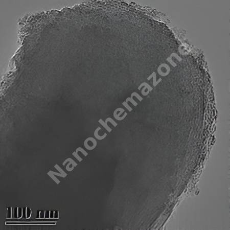
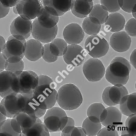
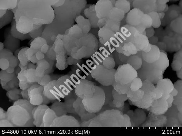
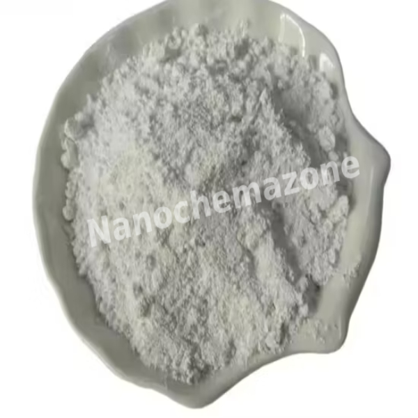
Niobium (Nb) Pentaoxide (Nb2O5) Nanoparticles, 100nm, >99.9% Purity, 100g

$286.00
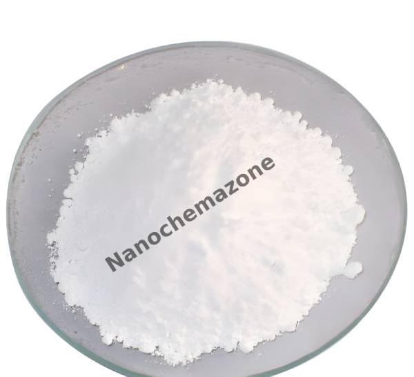
Product Niobium (Nb) Pentaoxide (Nb2O5) Nanoparticles, 100nm, >99.9% Purity, 100g
CAS No. 1313-96-8
Appearance Off-white to very light yellow
Purity ≥99%,  ≥99.9%,  ≥95%(Other purities are also available)
APS 100nm (Size Can be customized),  Ask for other available size range.
Ingredient Nb2O5
Molecular Weight 265.81 g/mol
Melting Point N/A
Boiling Point N/A
Density 4.47–4.60 g/cm³
Product Codes NCZ-477I

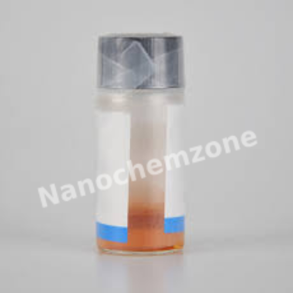
PLL (Polylysine) Coated Fe2O3 Nanoparticle Water Dispersion, 1mg/mL

Price range: $286.00 through $902.00
Select options This product has multiple variants. The options may be chosen on the product page
Product PLL (Polylysine) Coated Fe2O3 Nanoparticle Water Dispersion, 1mg/mL
CAS No. 1309-37-1
Appearance Dark reddish-brown colloidal suspension
Purity ≥99%,  ≥99.9%,  ≥95%(Other purities are also available)
APS 10–50nm (Size Can be customized),  Ask for other available size range.
Ingredient Fe₂O₃
Molecular Weight N/A
Melting Point N/A
Boiling Point N/A
Density 5.24 g/cm³
Product Codes NCZ-494I
 

Ultra Fine Magnetic Fe3O4 Nanoparticle for Biomolecular Coupling, 2-5nm

Price range: $286.00 through $539.00
Select options This product has multiple variants. The options may be chosen on the product page
Product Ultra Fine Magnetic Fe3O4 Nanoparticle for Biomolecular Coupling, 2-5nm
CAS No. 1317-61-9
Appearance Brown
Purity ≥99%,  ≥99.9%,  ≥95%(Other purities are also available)
APS 2-5nm (Size Can be customized),  Ask for other available size range.
Ingredient Fe3O4
Molecular Weight 231.53 g/mol
Melting Point N/A
Boiling Point N/A
Density 5.0–5.17 g/cm³
Product Codes NCZ-590I
 

Sodium hyaluronate(powder, Cosmetic grade) (335644)

$287.00
Select options This product has multiple variants. The options may be chosen on the product page
Sodium hyaluronate(powder, Cosmetic grade) (335644)

HA is a natural biotic component widely present in skin and other tissues. It has outstanding moisturizing effect, thus the name Natural Moisturizing Factor. HA is the best of its kind from nature for moisturizing in cosmetics.

  Applied to skin, macromolecular HA forms a thin layer permeable to air, keeping  skin smooth and moist and protecting it from bacteria, dust and ultraviolet rays, while micromolecular HA penetrates into corium, enlarging blood capillaries slightly, promoting blood circulation, improving intermediary metabolism and enhancing nutrient absorption to eliminate wrinkles, increase elasticity and delay aging. HA can also further hyperplasia of epidermic cells, clean oxygen-derived free radicals, prevent and rehabilitate skin injuries. Its aqueous solution has very high viscosity, while cream made by emulsifying HA with oil is fine and even.   HA can be added to almost any cosmetics, such as cream, lotion, astringent, essence, facial cleanser, shower gel, shampoo, hair conditioner, mousse and lip stick. In most cases, the dosage is around 0.05%-0.5%.   Characteristics  White or off-white powder, hygroscopic, odorless. Specifications  
pH(1% water solution) 6.0-7.5
Transparency ≥99.0%
Loss on drying ≤10.0%
Kinematic viscosity as measured
Molecular weight 500,000-2,000,000
Protein ≤0.1%
Heavy metals(as Pb) ≤20ug/g
 Assay
Glucuronic Acid ≥44.0%
Sodium Hyaluronate ≥91.0%
 Microbial Examination
Bacteria counts 10cfu/g
Mold&Yeast 10cfu/g
Staphylococcus aureus negative
Pseudomonas aeruginosa negative
 
Product Codes- NCZ-2702K

Gadolinium (Gd) Micron Powder, Purity: 99.5 %, Size: 325 mesh

Price range: $288.00 through $1,538.00
Select options This product has multiple variants. The options may be chosen on the product page
25 grams/288 € 100 grams/893 € 500 grams/ 1538 €   Please contact us for quotes on larger quantities !!! Gadolinium (Gd) Micron Powder

Molybdenum (Mo) Sputtering Targets, Purity: 99.95%, Size: 8”, Thickness: 0.250”

$288.00

Applications of Sputtering Targets;

For film deposition, sputtering targets are employed. A sputtering technique called "deposition made by sputter targets" entails eroding material from a "target" source onto a "substrate" like a silicon wafer. Targets are etched using semiconductor sputtering targets. When etching anisotropy is required to a great degree and selectivity is not an issue, sputter etching is the method of choice. By etching away the target material, sputter targets are also utilized for investigation. In one instance, the target sample is sputtered at a steady pace in secondary ion spectroscopy (SIMS). Using mass spectrometry, the concentration and identity of the spewed atoms are determined when the target is sputtered.

By helping of the sputtering target, the composition of the target material may be evaluated and even extremely tiny amounts of contaminants are recognized.

There is also an application area for sputtering targets in space. One type of space weathering that alters the chemical and physical characteristics of airless worlds like the Moon and asteroids is sputtering.

Selenium (Se) Sputtering Targets, Purity: 99.999%, Size: 3”, Thickness: 0.125”

$288.00

Applications of Sputtering Targets;

Film deposition is accomplished using sputtering targets. A technique for sputtering thin films is called "deposition made by sputter targets," which entails eroding material from a "target" source onto a "substrate" like a silicon wafer. Etching of the target is done using semiconductor sputtering targets. When selectivity is not an issue and a high degree of etching anisotropy is required, sputter etching is the method of choice. By removing the target material through etching, sputter targets are also utilized for investigation. In secondary ion spectroscopy (SIMS), one example is when the target material is sputtered at a steady pace. Mass spectrometry is used to quantify the concentration and identity of spewed atoms as the target is sputtered.

The target material's composition may be ascertained and even very low concentrations of contaminants can be found with the aid of the sputtering target.

There is also an application area for sputtering targets in space. One type of space weathering that alters the chemical and physical characteristics of airless worlds like the Moon and asteroids is sputtering.

Copper Sputtering Target Cu

Price range: $288.00 through $585.00
Select options This product has multiple variants. The options may be chosen on the product page
Product Copper Sputtering Target Cu
CAS No. 7440-50-8
Appearance Solid, reddish-orange metallic luster
Purity ≥99%,  ≥99.9%,  ≥95% (Other purities are also available)
APS N/A
Ingredient Cu
Molecular Weight 63.55 g/mol
Melting Point 1083.0 °C
Boiling Point 2567.0 °C
Density 8.96 g/cm³
Product Codes NCZ-113H

Boron Nitride (BN) Sputtering Target

Price range: $288.00 through $852.00
Select options This product has multiple variants. The options may be chosen on the product page

Product 

Boron Nitride (BN) Sputtering Target

CAS No.

10043-11-5

Appearance

Powder

Purity

≥99%,  ≥99.9%,  ≥95%

(Other purities are also available)

APS

 NA (Size Can be customized), Ask for other available size ranges.

Ingredient

N/A

Molecular Weight

24.82 g/mol

Melting Point

~2,973 °C

Boiling Point

N/A

Density

 ~2.1–3.5 g/cm³

Product Codes

NCZ-1333K

Silicon Dioxide (SiO2) Sputtering Targets, Fused Quartz, Purity: 99.995%, Size: 6”, Thickness: 0.250”

$288.00

Product 

Silicon Dioxide (SiO2) Sputtering Targets, Fused Quartz, Purity: 99.995%, Size: 6'', Thickness: 0.250''

CAS No.

7631-86-9

Appearance

Powder

Purity

≥99%,  ≥99.9%,  ≥95%

(Other purities are also available)

APS

N/A  (Size Can be customized), Ask for other available size ranges.

Ingredient

N/A

Molecular Weight

60.08 g/mol

Melting Point

~1710°C

Boiling Point

 ~2,950 °C

Density

~2.20 g/cm³

Product Codes

NCZ-1711K

Indium Zinc Oxide/IZO (InZnO) Sputtering Targets, Purity: 99.99%, Size: 1”, Thickness: 0.125”

$288.00

Product 

Indium Zinc Oxide/IZO (InZnO) Sputtering Targets, Purity: 99.99%, Size: 1'', Thickness: 0.125''

CAS No.

Indium oxide (In₂O₃): 1312-43-2
Zinc oxide (ZnO): 1314-13-2

Appearance

Powder

Purity

≥99%,  ≥99.9%,  ≥95%

(Other purities are also available)

APS

 N/A (Size Can be customized), Ask for other available size ranges.

Ingredient

N/A

Molecular Weight

Approx. 260–270 g/mol (depends on ratio)

Melting Point

Indium oxide: ~1910 °C Zinc oxide: ~1975 °C

Boiling Point

N/A

Density

~7.1 g/cm³

Product Codes

NCZ-2201K

Indium Oxide (In2O3) Sputtering Targets, Purity: 99.99%, Size: 1”, Thickness: 0.250”

$288.00

Product 

Indium Oxide (In2O3) Sputtering Targets, Purity: 99.99%, Size: 1'', Thickness: 0.250''

CAS No.

 1312-43-2

Appearance

Powder

Purity

≥99%,  ≥99.9%,  ≥95%

(Other purities are also available)

APS

< 5 µm (Size Can be customized), Ask for other available size ranges.

Ingredient

N/A

Molecular Weight

 277.64 g/mol

Melting Point

 ~1,910 °C

Boiling Point

 3,000 °C(approx., decomposes)

Density

~7.18 g/cm³ (sintered form)

Product Codes

NCZ-2219K

Bismuth (Bi) Sputtering Targets, Purity: 99.9%, Size: 4”, Thickness: 0.250”

$288.00

Product 

Bismuth (Bi) Sputtering Targets, Purity: 99.9%, Size: 4'', Thickness: 0.250''

CAS No.

7440‑69‑9

Appearance

Powder

Purity

≥99%,  ≥99.9%,  ≥95%

(Other purities are also available)

APS

1 – 5 µm (Size Can be customized), Ask for other available size ranges.

Ingredient

N/A

Molecular Weight

208.98 amu (~208.98 g/mol)

Melting Point

 271.4 °C

Boiling Point

~1560 °C

Density

 ~9.78–9.80 g/cm³

Product Codes

NCZ-2432K

Aluminum Silicon (AlSi) Sputtering Targets, Purity: 99.999%, Size: 4”, Thickness: 0.250”

$288.00

Product 

Aluminum Silicon (AlSi) Sputtering Targets, Purity: 99.999%, Size: 4'', Thickness: 0.250''

CAS No.

Aluminum: 7429-90-5 Silicon: 7440-21-3

Appearance

Powder

Purity

≥99%,  ≥99.9%,  ≥95%

(Other purities are also available)

APS

N/A (Size Can be customized), Ask for other available size ranges.

Ingredient

N/A

Molecular Weight

 Depends on alloy ratio (Al = 26.98, Si = 28.09)

Melting Point

 ~577–660 °C (depends on Si content)

Boiling Point

~2519 °C (approx.)

Density

~2.6–2.7 g/cm³

Product Codes

NCZ-2512K

Nickel (Ni) Sputtering Targets, Purity: 99.99%, Size: 5”, Thickness: 0.250”

$289.00

Applications of Sputtering Targets;

Film deposition is accomplished using sputtering targets. A technique for sputtering thin films is called "deposition made by sputter targets," which entails eroding material from a "target" source onto a "substrate" like a silicon wafer. Etching of the target is done using semiconductor sputtering targets. When selectivity is not an issue and a high degree of etching anisotropy is required, sputter etching is the method of choice. By removing the target material through etching, sputter targets are also utilized for investigation. In secondary ion spectroscopy (SIMS), one example is when the target material is sputtered at a steady pace. Mass spectrometry is used to quantify the concentration and identity of spewed atoms as the target is sputtered.

The target material's composition may be ascertained and even very low concentrations of contaminants can be found with the aid of the sputtering target.

There is also an application area for sputtering targets in space. One type of space weathering that alters the chemical and physical characteristics of airless worlds like the Moon and asteroids is sputtering.

Aminated Graphene Quantum Dots Solution, 1mg/mL

Price range: $289.00 through $489.00
Select options This product has multiple variants. The options may be chosen on the product page
Product Aminated Graphene Quantum Dots Solution, 1mg/mL
CAS No. N/A
Appearance Clear to light yellow or pale brown
Purity ≥99%,  ≥99.9%,  ≥95%(Other purities are also available)
APS 2-10nm (Size Can be customized),  Ask for other available size range.
Ingredient C₁₀₀H₄₀N₅O₁₀
Molecular Weight N/A
Melting Point N/A
Boiling Point N/A
Density N/A
Product Codes NCZ-284I
 

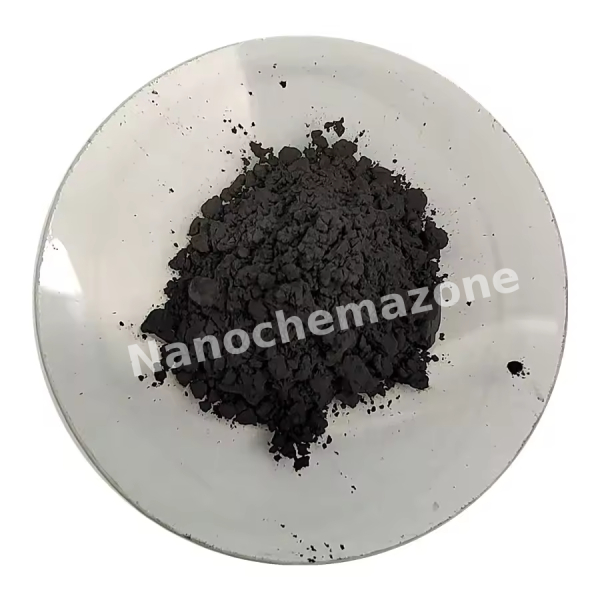
Niobium Aluminum Carbide (Nb2AlC) MAX Phase Micron-Powder

Price range: $289.00 through $889.00
Select options This product has multiple variants. The options may be chosen on the product page
Product Niobium Aluminum Carbide (Nb2AlC) MAX Phase Micron-Powder
CAS No. 60687-94-7
Appearance Gray-black to black
Purity ≥99%,  ≥99.9%,  ≥95%(Other purities are also available)
APS  0.8–30µm (Size Can be customized),  Ask for other available size range.
Ingredient Nb2AlC
Molecular Weight 224.8 g/mol
Melting Point N/A
Boiling Point N/A
Density 6.43 g/cm³
Product Codes NCZ-479I

Selenium (Se) Sputtering Targets, Purity: 99.999%, Size: 4”, Thickness: 0.125”

$290.00

Applications of Sputtering Targets;

Film deposition is accomplished using sputtering targets. A technique for sputtering thin films is called "deposition made by sputter targets," which entails eroding material from a "target" source onto a "substrate" like a silicon wafer. Etching of the target is done using semiconductor sputtering targets. When selectivity is not an issue and a high degree of etching anisotropy is required, sputter etching is the method of choice. By removing the target material through etching, sputter targets are also utilized for investigation. In secondary ion spectroscopy (SIMS), one example is when the target material is sputtered at a steady pace. Mass spectrometry is used to quantify the concentration and identity of spewed atoms as the target is sputtered.

The target material's composition may be ascertained and even very low concentrations of contaminants can be found with the aid of the sputtering target.

There is also an application area for sputtering targets in space. One type of space weathering that alters the chemical and physical characteristics of airless worlds like the Moon and asteroids is sputtering.

Silver (Ag) Sputtering Targets, Purity: 99.99%, Size: 2”, Thickness: 0.125”

$290.00

Product 

Silver (Ag) Sputtering Targets, Purity: 99.99%, Size: 2'', Thickness: 0.125''

CAS No.

 7440-22-4

Appearance

Powder

Purity

≥99%,  ≥99.9%,  ≥95%

(Other purities are also available)

APS

N/A  (Size Can be customized), Ask for other available size ranges.

Ingredient

N/A

Molecular Weight

107.87 g/mol

Melting Point

 961.78 °C

Boiling Point

 2162 °C

Density

 10.49 g/cm³

Product Codes

NCZ-1692K

Copper (Cu) Sputtering Targets, Purity: 99.99%, Size: 7”, Thickness: 0.125”

$290.00

Product 

Copper (Cu) Sputtering Targets, Purity: 99.99%, Size: 7'', Thickness: 0.125''

CAS No.

7440-50-8

Appearance

Powder

Purity

≥99%,  ≥99.9%,  ≥95%

(Other purities are also available)

APS

 N/A (Size Can be customized), Ask for other available size ranges.

Ingredient

N/A

Molecular Weight

63.55 g/mol

Melting Point

1,084 °C

Boiling Point

 2,562 °C

Density

8.96 g/cm³

Product Codes

NCZ-2255K

H-MCM-41(Pore Diameter=8nm) (936853)

$290.00
Select options This product has multiple variants. The options may be chosen on the product page
H-MCM-41(Pore Diameter=8nm) (936853)

Pore Diameter 8 nm SiO2/Al2O3 20-50, 50-100, 100-200, All Si Relative Crystallinity 95% Na2O <1000 ppm Loss on Ignition <5% 

Product Codes- NCZ-2720K

H-MCM-41(Pore Diameter=3.8nm) (936940)

$290.00
Select options This product has multiple variants. The options may be chosen on the product page
H-MCM-41(Pore Diameter=3.8nm) (936940)

Pore Diameter 3.8nm SiO2/Al2O3 25, All Si Surface area 1000m2/g D50 1.2µm

Product Codes- NCZ-2721K

H-MCM-48(All Si) (883853)

$290.00
Select options This product has multiple variants. The options may be chosen on the product page
H-MCM-48(All Si) (883853)

Pore Structure three-dimensional spiral Pore Size(nm) 3.0 - 4.0 SiO2/Al2O3 All Si Relative Crystallinity(%) > 90 Na2O weight(%) <= 0.1

Product Codes- NCZ-2722K

H-ZSM-5 (293853)

$290.00
Select options This product has multiple variants. The options may be chosen on the product page
H-ZSM-5 (293853)

Pore Structure  MFI Pore Size(nm)  0.53 - 0.58   SiO2/Al2O3   15 - 45, 45 - 80, 80 - 150, 150 - 300 Relative Crystallinity(%)   >= 95 Na2O weight(%)  <= 0.1 Loss on Ignition(%)  <= 5 

Product Codes- NCZ-2723K

H-ZSM-11 (277853)

$290.00
Select options This product has multiple variants. The options may be chosen on the product page
H-ZSM-11 (277853)

Pore Structure  MEL Pore Size(nm)  0.56 - 0.58   SiO2/Al2O3   15 - 45, 45 - 80, 80 - 150, 150 - 300 Relative Crystallinity(%)   >= 95 Na2O weight(%)  <= 0.1 Loss on Ignition(%)  <= 5 

Product Codes- NCZ-2724K

H-ZSM-12 (268853)

$290.00
Select options This product has multiple variants. The options may be chosen on the product page
H-ZSM-12 (268853)

Pore Structure  MTW Pore Size(nm)  SiO2/Al2O3   20 - 60, 60 - 150 Relative Crystallinity(%)   >= 95 Na2O weight(%)  <= 0.1 Loss on Ignition(%)  <= 5

 
Product Codes- NCZ-2725K

K-ZSM-22 (255853)

$290.00
Select options This product has multiple variants. The options may be chosen on the product page
K-ZSM-22 (255853)

Pore Structure  TON Pore Size(nm)  0.55 - 0.80  SiO2/Al2O3  40 - 80, 80 - 150, 150 - 300 Relative Crystallinity(%)   >= 95 Loss on Ignition(%)  <= 5 

 
Product Codes- NCZ-2727K

H-ZSM-23(SiO2/Al2O3≥500) (239853)

$290.00
Select options This product has multiple variants. The options may be chosen on the product page
H-ZSM-23(SiO2/Al2O3≥500) (239853)

Pore Structure  MTT Pore Size(nm)  SiO2/Al2O3  >= 500 Relative Crystallinity(%)   >= 95 Na2O weight(%)  <= 0.1 Loss on Ignition(%)  <= 5 

 
Product Codes- NCZ-2728K

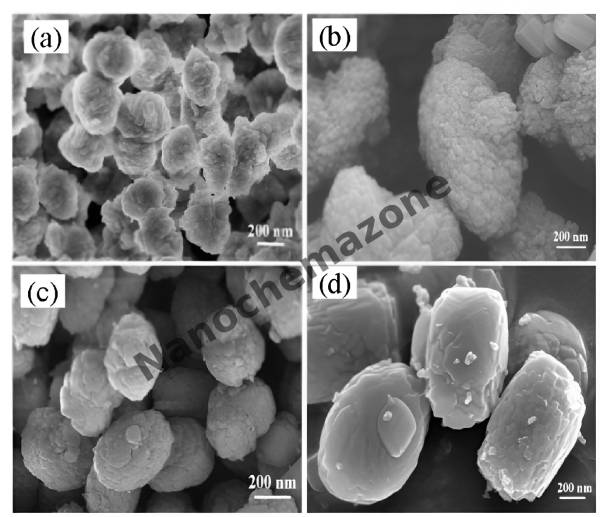
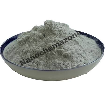
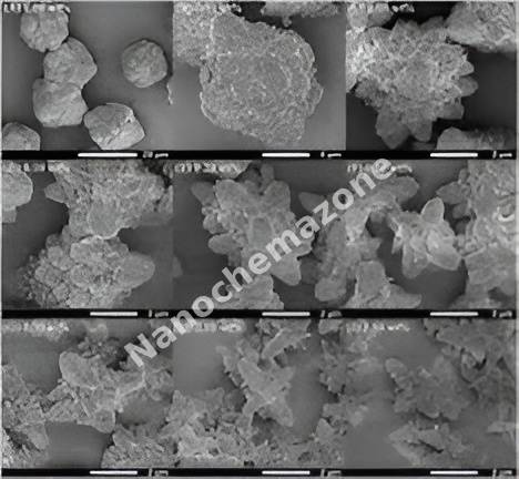
H-ZSM-35 (232853)

$290.00
Select options This product has multiple variants. The options may be chosen on the product page
H-ZSM-35 (232853)

Pore Structure  FER Pore Size(nm)  0.5 - 0.6 SiO2/Al2O3  10 - 20, 20 - 40, 40 - 60   Relative Crystallinity(%)   >= 95 Na2O weight(%)  <= 0.1 Loss on Ignition(%)  <= 5 

Product Codes- NCZ-2729K

H-ZSM-48(SiO2/Al2O3≥500) (228853)

$290.00
Select options This product has multiple variants. The options may be chosen on the product page
H-ZSM-48(SiO2/Al2O3≥500) (228853)

Pore Structure  MRE SiO2/Al2O3  >= 500 Relative Crystallinity(%)   >= 95 Na2O weight(%)  <= 0.1 Loss on Ignition(%)  <= 5


Product Codes- NCZ-2730K

SAPO-5(SiO2/Al2O3=0.3-0.5) (978853)

$290.00
Select options This product has multiple variants. The options may be chosen on the product page
SAPO-5(SiO2/Al2O3=0.3-0.5) (978853)

Pore Structure AFI SiO2/Al2O3 0.3 - 0.5 Relative Crystallinity(%) >= 95 Na2O weight(%) < 0.1 Loss on Ignition(%) < 5 


Product Codes- NCZ-2731K

SAPO-11 (972853)

$290.00
SAPO-11 (972853)

Pore Structure AEL Pore Size(nm) 0.6 - 0.7 SiO2/P2O5/Al2O3 = 0-0.3 : 1 : 1, 0.3-0.5 : 1 : 1, 0.5-0.8 : 1 : 1 Relative Crystallinity(%) >= 95 Na2O weight(%) <= 0.1 Loss on Ignition(%) <= 5 


Product Codes- NCZ-2732K

SAPO-34(SiO2/P2O5/Al2O3=0.4:1:1) (963853)

$290.00
Select options This product has multiple variants. The options may be chosen on the product page
SAPO-34(SiO2/P2O5/Al2O3=0.4:1:1) (963853)

Pore Structure CHA SiO2/P2O5/Al2O3 = 0.4 : 1 : 1 Relative Crystallinity(%) >= 95 Na2O weight(%) <= 0.1 Loss on Ignition(%) <= 5    


Product Codes- NCZ-2733K

SAPO-35 (961853)

$290.00
SAPO-35 (961853)

Pore Structure LEV Pore Size(nm) 0.7 - 1.7

SiO2/Al2O3 0 - 0.3 

SiO2/Al2O3 0.3 - 0.8

SiO2/Al2O3 0.8 - 1.2

Relative Crystallinity(%) >= 95 Na2O weight(%) <= 0.1 Loss on Ignition(%) <= 5


Product Codes- NCZ-2734K

SAPO-37(SiO2/P2O5/Al2O3=0-0.3:1:1) (254853)

$290.00
Select options This product has multiple variants. The options may be chosen on the product page
SAPO-37(SiO2/P2O5/Al2O3=0-0.3:1:1) (254853)
Framework Type FAU Pore Size(nm) 0.8 SiO2/P2O5/Al2O3 = 0-0.3 : 1 : 1 Relative Crystallinity(%) >= 95 Loss on Ignition(%) <= 5


Product Codes- NCZ-2735K

SAPO-41(SiO2/P2O5/Al2O3=0-0.3:1:1) (557853)

$290.00
Select options This product has multiple variants. The options may be chosen on the product page
SAPO-41(SiO2/P2O5/Al2O3=0-0.3:1:1) (557853)
Framework Type AFO SiO2/P2O5/Al2O3 = 0-0.3 : 1 : 1 Relative Crystallinity(%) >= 95 Loss on Ignition(%) <= 5


Product Codes- NCZ-2736K

SAPO-42(SiO2/P2O5/Al2O3=0-0.3:1:1) (355853)

$290.00
Select options This product has multiple variants. The options may be chosen on the product page
SAPO-42(SiO2/P2O5/Al2O3=0-0.3:1:1) (355853)
Framework Type LTA Pore Size(nm) 0.43 SiO2/P2O5/Al2O3 = 0-0.3 : 1 : 1 Relative Crystallinity(%) >= 95 Loss on Ignition(%) <= 5


Product Codes- NCZ-2738K

SAPO-46(SiO2/P2O5/Al2O3=0.2:1:1.3) (976853)

$290.00
Select options This product has multiple variants. The options may be chosen on the product page
SAPO-46(SiO2/P2O5/Al2O3=0.2:1:1.3) (976853)

SiO2/P2O5/Al2O3 = 0.2 : 1 : 1.3 Relative Crystallinity(%) >= 95 Na2O weight(%) <= 0.1 Loss on Ignition(%) <= 5 


Product Codes- NCZ-2739K

SAPO-47(SiO2/P2O5/Al2O3=0.3:1:1) (977853)

$290.00
Select options This product has multiple variants. The options may be chosen on the product page
SAPO-47(SiO2/P2O5/Al2O3=0.3:1:1) (977853)

Pore Structure CHA SiO2/P2O5/Al2O3 = 0.3 : 1 : 1 Relative Crystallinity(%) >= 95 Na2O weight(%) <= 0.1 Loss on Ignition(%) <= 5 


Product Codes- NCZ-2740K

Aluminum (Al) Sputtering Targets, Purity: 99.999%, Size: 4”, Thickness: 0.125”

$291.00

Applications of Sputtering Targets;

  • Sputtering targets is used for film deposition. The deposition made by sputter targets is a method of depositing thin films by sputtering that involves eroding material from a "target" source onto a "substrate" such as  a silicon wafer.
  • Semiconductor sputtering targets is used to etch the target. Sputter etching is chosen in cases where a high degree of etching anisotropy is needed and selectivity is not a concern.
  • Sputter targets is also used for analysis by etching away the target material.
One of the example occurs in secondary ion spectroscopy (SIMS), where the target sample is sputtered at a constant rate. As the target is sputtered, the concentration and identity of sputtered atoms are measured using mass spectrometry. By helping of the sputtering target, the composition of the target material can be determined and even extremely low concentrations of impurities are detected. Sputtering target has also application area in space. Sputtering is one of the forms of space weathering, a process that changes the physical and chemical properties of airless bodies, such as asteroids and the Moon. Aluminum which has the chemical symbol of Al, is a silvery white, soft, ductile metal that is the third most abundant element. Aluminum is notable due to for its light weight, strength, durability and for its ability to resist corrosion. Aluminum forms an extremely thin but very strong layer of oxide film. Aluminum has also high thermal and electrical conductivity. Aluminum sputtering targets have a particularly fine-grained microstructure. This property of Aluminum sputtering targets ensures that you benefit from uniform erosion and a low susceptibility to particle formation throughout the sputtering process.

Vanadium (V) Sputtering Targets, Purity: 99.5%, Size: 3”, Thickness: 0.125”

$291.00

Applications of Sputtering Targets;

Film deposition is accomplished using sputtering targets. A technique for sputtering thin films is called "deposition made by sputter targets," which entails eroding material from a "target" source onto a "substrate" like a silicon wafer. Etching of the target is done using semiconductor sputtering targets. When selectivity is not an issue and a high degree of etching anisotropy is required, sputter etching is the method of choice. By removing the target material through etching, sputter targets are also utilized for investigation. In secondary ion spectroscopy (SIMS), one example is when the target material is sputtered at a steady pace. Mass spectrometry is used to quantify the concentration and identity of spewed atoms as the target is sputtered.

The target material's composition may be ascertained and even very low concentrations of contaminants can be found with the aid of the sputtering target.

There is also an application area for sputtering targets in space. One type of space weathering that alters the chemical and physical characteristics of airless worlds like the Moon and asteroids is sputtering.

Tantalum (Ta) Sputtering Targets, Purity: 99.95%, Size: 2”, Thickness: 0.250”

$291.00

Product 

Tantalum (Ta) Sputtering Targets, Purity: 99.95%, Size: 2'', Thickness: 0.250''

CAS No.

 7440-25-7

Appearance

Powder

Purity

≥99%,  ≥99.9%,  ≥95%

(Other purities are also available)

APS

N/A  (Size Can be customized), Ask for other available size ranges.

Ingredient

N/A

Molecular Weight

 180.95 g/mol

Melting Point

3017 °C

Boiling Point

 5458 °C

Density

16.65 g/cm³

Product Codes

NCZ-1664K

Cerium Chloride Heptahydrate (CeCl3 · 7H2O) 99.9% 3N

$291.00
Select options This product has multiple variants. The options may be chosen on the product page
Product Cerium Chloride Heptahydrate (CeCl3 · 7H2O) 99.9% 3N
CAS No. 7790-91-2
Appearance Pale green to white crystalline
Purity ≥99%,  ≥99.9%,  ≥95%(Other purities are also available)
APS N/A
Ingredient CeCl3·7H2O
Molecular Weight 372.58 g/mol
Melting Point N/A
Boiling Point N/A
Density 1.98 g/cm³
Product Codes NCZ-314I
 

Sodium Carbonate (Na2CO3) 99.999% 5N High Purity Powder

$291.00
Select options This product has multiple variants. The options may be chosen on the product page
Product Sodium Carbonate (Na2CO3) 99.999% 5N High Purity Powder
CAS No. 497-19-8
Appearance White, odorless crystalline or fine
Purity ≥99%,  ≥99.9%,  ≥95%(Other purities are also available)
APS 1–10µm (Size Can be customized),  Ask for other available size range.
Ingredient Na2CO3
Molecular Weight 105.99 g/mol
Melting Point 851 °C
Boiling Point N/A
Density 2.54 g/cm³
Product Codes NCZ-528I
 

Impending Self-Help Transfer Nickel Graphene Foam, Thickness: 1±0.1 mm, Size: 2×2 cm

Price range: $292.00 through $1,348.00
Select options This product has multiple variants. The options may be chosen on the product page
1 piece/ 292 € 5 pieces/ 1348 €  Contact us for tailored quotes on larger quantities & experience exceptional solutions from our

Barium (Ba) Sputtering Targets, Purity: 99.5%, Size: 2”, Thickness: 0.250”

$292.00

Applications of Sputtering Targets;

Film deposition is accomplished using sputtering targets. A technique for sputtering thin films is called "deposition made by sputter targets," which entails eroding material from a "target" source onto a "substrate" like a silicon wafer. Etching of the target is done using semiconductor sputtering targets. When selectivity is not an issue and a high degree of etching anisotropy is required, sputter etching is the method of choice. By removing the target material through etching, sputter targets are also utilized for investigation. In secondary ion spectroscopy (SIMS), one example is when the target material is sputtered at a steady pace. Mass spectrometry is used to quantify the concentration and identity of spewed atoms as the target is sputtered. With the sputtering target's assistance, theFilm deposition is accomplished using sputtering targets. A technique for sputtering thin films is called "deposition made by sputter targets," which entails eroding material from a "target" source onto a "substrate" like a silicon wafer. Etching of the target is done using semiconductor sputtering targets. When selectivity is not an issue and a high degree of etching anisotropy is required, sputter etching is the method of choice. By removing the target material through etching, sputter targets are also utilized for investigation. In secondary ion spectroscopy (SIMS), one example is when the target material is sputtered at a steady pace. Mass spectrometry is used to quantify the concentration and identity of spewed atoms as the target is sputtered. With the sputtering target's assistance, theFilm deposition is accomplished using sputtering targets. A technique for sputtering thin films is called "deposition made by sputter targets," which entails eroding material from a "target" source onto a "substrate" like a silicon wafer. Etching of the target is done using semiconductor sputtering targets. When selectivity is not an issue and a high degree of etching anisotropy is required, sputter etching is the method of choice. By removing the target material through etching, sputter targets are also utilized for investigation. In secondary ion spectroscopy (SIMS), one example is when the target material is sputtered at a steady pace. Mass spectrometry is used to quantify the concentration and identity of spewed atoms as the target is sputtered. With the sputtering target's assistance, theFilm deposition is accomplished using sputtering targets. A technique for sputtering thin films is called "deposition made by sputter targets," which entails eroding material from a "target" source onto a "substrate" like a silicon wafer. Etching of the target is done using semiconductor sputtering targets. When selectivity is not an issue and a high degree of etching anisotropy is required, sputter etching is the method of choice. By removing the target material through etching, sputter targets are also utilized for investigation. In secondary ion spectroscopy (SIMS), one example is when the target material is sputtered at a steady pace. Mass spectrometry is used to quantify the concentration and identity of spewed atoms as the target is sputtered. With the sputtering target's assistance, theFilm deposition is accomplished using sputtering targets. A technique for sputtering thin films is called "deposition made by sputter targets," which entails eroding material from a "target" source onto a "substrate" like a silicon wafer. Etching of the target is done using semiconductor sputtering targets. When selectivity is not an issue and a high degree of etching anisotropy is required, sputter etching is the method of choice. By removing the target material through etching, sputter targets are also utilized for investigation. In secondary ion spectroscopy (SIMS), one example is when the target material is sputtered at a steady pace. Mass spectrometry is used to quantify the concentration and identity of spewed atoms as the target is sputtered. With the sputtering target's assistance, theFilm deposition is accomplished using sputtering targets. A technique for sputtering thin films is called "deposition made by sputter targets," which entails eroding material from a "target" source onto a "substrate" like a silicon wafer. Etching of the target is done using semiconductor sputtering targets. When selectivity is not an issue and a high degree of etching anisotropy is required, sputter etching is the method of choice. By removing the target material through etching, sputter targets are also utilized for investigation. In secondary ion spectroscopy (SIMS), one example is when the target material is sputtered at a steady pace. Mass spectrometry is used to quantify the concentration and identity of spewed atoms as the target is sputtered. With the sputtering target's assistance, theFilm deposition is accomplished using sputtering targets. A technique for sputtering thin films is called "deposition made by sputter targets," which entails eroding material from a "target" source onto a "substrate" like a silicon wafer. Etching of the target is done using semiconductor sputtering targets. When selectivity is not an issue and a high degree of etching anisotropy is required, sputter etching is the method of choice. By removing the target material through etching, sputter targets are also utilized for investigation. In secondary ion spectroscopy (SIMS), one example is when the target material is sputtered at a steady pace. Mass spectrometry is used to quantify the concentration and identity of spewed atoms as the target is sputtered. With the sputtering target's assistance, theFilm deposition is accomplished using sputtering targets. A technique for sputtering thin films is called "deposition made by sputter targets," which entails eroding material from a "target" source onto a "substrate" like a silicon wafer. Etching of the target is done using semiconductor sputtering targets. When selectivity is not an issue and a high degree of etching anisotropy is required, sputter etching is the method of choice. By removing the target material through etching, sputter targets are also utilized for investigation. In secondary ion spectroscopy (SIMS), one example is when the target material is sputtered at a steady pace. Mass spectrometry is used to quantify the concentration and identity of spewed atoms as the target is sputtered. With the sputtering target's assistance, theFilm deposition is accomplished using sputtering targets. A technique for sputtering thin films is called "deposition made by sputter targets," which entails eroding material from a "target" source onto a "substrate" like a silicon wafer. Etching of the target is done using semiconductor sputtering targets. When selectivity is not an issue and a high degree of etching anisotropy is required, sputter etching is the method of choice. By removing the target material through etching, sputter targets are also utilized for investigation. In secondary ion spectroscopy (SIMS), one example is when the target material is sputtered at a steady pace. Mass spectrometry is used to quantify the concentration and identity of spewed atoms as the target is sputtered. With the sputtering target's assistance, theFilm deposition is accomplished using sputtering targets. A technique for sputtering thin films is called "deposition made by sputter targets," which entails eroding material from a "target" source onto a "substrate" like a silicon wafer. Etching of the target is done using semiconductor sputtering targets. When selectivity is not an issue and a high degree of etching anisotropy is required, sputter etching is the method of choice. By removing the target material through etching, sputter targets are also utilized for investigation. In secondary ion spectroscopy (SIMS), one example is when the target material is sputtered at a steady pace. Mass spectrometry is used to quantify the concentration and identity of spewed atoms as the target is sputtered. With the sputtering target's assistance, theFilm deposition is accomplished using sputtering targets. A technique for sputtering thin films is called "deposition made by sputter targets," which entails eroding material from a "target" source onto a "substrate" like a silicon wafer. Etching of the target is done using semiconductor sputtering targets. When selectivity is not an issue and a high degree of etching anisotropy is required, sputter etching is the method of choice. By removing the target material through etching, sputter targets are also utilized for investigation. In secondary ion spectroscopy (SIMS), one example is when the target material is sputtered at a steady pace. Mass spectrometry is used to quantify the concentration and identity of spewed atoms as the target is sputtered. With the sputtering target's assistance, theFilm deposition is accomplished using sputtering targets. A technique for sputtering thin films is called "deposition made by sputter targets," which entails eroding material from a "target" source onto a "substrate" like a silicon wafer. Etching of the target is done using semiconductor sputtering targets. When selectivity is not an issue and a high degree of etching anisotropy is required, sputter etching is the method of choice. By removing the target material through etching, sputter targets are also utilized for investigation. In secondary ion spectroscopy (SIMS), one example is when the target material is sputtered at a steady pace. Mass spectrometry is used to quantify the concentration and identity of spewed atoms as the target is sputtered. With the sputtering target's assistance, theFilm deposition is accomplished using sputtering targets. A technique for sputtering thin films is called "deposition made by sputter targets," which entails eroding material from a "target" source onto a "substrate" like a silicon wafer. Etching of the target is done using semiconductor sputtering targets. When selectivity is not an issue and a high degree of etching anisotropy is required, sputter etching is the method of choice. By removing the target material through etching, sputter targets are also utilized for investigation. In secondary ion spectroscopy (SIMS), one example is when the target material is sputtered at a steady pace. Mass spectrometry is used to quantify the concentration and identity of spewed atoms as the target is sputtered. With the sputtering target's assistance, the

It is possible to identify the target material and even detect incredibly tiny impurity amounts.

There is also an application area for sputtering targets in space. One type of space weathering that alters the chemical and physical characteristics of airless worlds like the Moon and asteroids is sputtering.

A Block S, Group 2, Period 6 element with an atomic weight of 137.27, barium has the atomic symbol Ba and atomic number 56. One of the alkaline-earth metals is barium. Electronics can be plated using barium sputtering targets. Barium has favorable electrical characteristics.

Barium (Ba) Sputtering Targets, Purity: 99.5%, Size: 2”, Thickness: 0.125”

$292.00

Applications of Sputtering Targets;

Film deposition is accomplished using sputtering targets. A technique for sputtering thin films is called "deposition made by sputter targets," which entails eroding material from a "target" source onto a "substrate" like a silicon wafer. Etching of the target is done using semiconductor sputtering targets. When selectivity is not an issue and a high degree of etching anisotropy is required, sputter etching is the method of choice. By removing the target material through etching, sputter targets are also utilized for investigation. In secondary ion spectroscopy (SIMS), one example is when the target material is sputtered at a steady pace. Mass spectrometry is used to quantify the concentration and identity of spewed atoms as the target is sputtered. With the sputtering target's assistance, the

It is possible to identify the target material and even detect incredibly tiny impurity amounts.

There is also an application area for sputtering targets in space. One type of space weathering that alters the chemical and physical characteristics of airless worlds like the Moon and asteroids is sputtering.

A Block S, Group 2, Period 6 element with an atomic weight of 137.27, barium has the atomic symbol Ba and atomic number 56. One of the alkaline-earth metals is barium. Electronics can be plated using barium sputtering targets. Barium is beneficial for sputtering applications because of its good electrical characteristics. Barium sputtering targets can be utilized for semiconductors. Barium for flat panel screens

Chitosan Oligosaccharide(from Mushroom) (238555)

$292.00
Select options This product has multiple variants. The options may be chosen on the product page
Chitosan Oligosaccharide(from Mushroom) (238555)
ANALYSIS SPECIFICATION RUSULT
Deacetylation ≥98% 98.2%
Appearance Light yellow -brown powder Complies
pH 5.5-7 5.7
Mesh size 150mesh 100% pass 150 mesh
Molecular weight ≤5500Da 5100Da
Moisture ≤10% 5.1%
Total ash ≤ 2% 0.45%
Heavy Metals ≤ 10 ppm 6ppm
As ≤ 2.0ppm 1ppm
Pb ≤ 1.0ppm 0.5ppm
Cd ≤ 0.5ppm Negative
Hg ≤ 0.5ppm Negative
Microbiological quality Total Plate Count Yeast & Mold E.Coliform Salmonella . <1000cfu/g <100cfu/g Negative Negative . 200cfu/g 50cfu/g Negative Negative
  Product Codes- NCZ-2663K

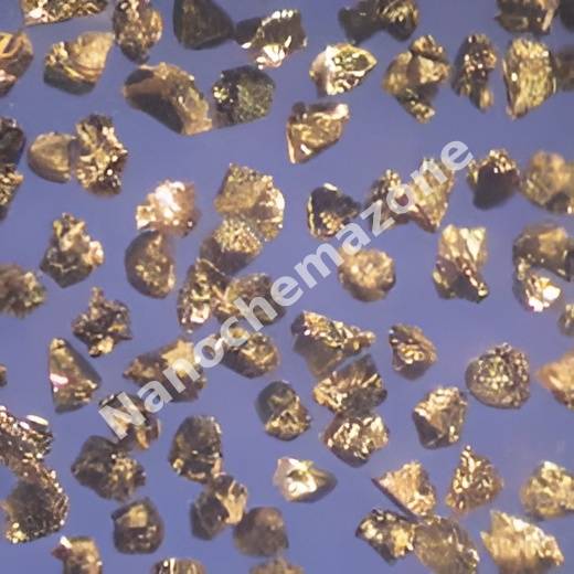
Cubic Boron nitride(CBN, mono-crystal) (322514)

$292.00
Cubic Boron nitride(CBN, mono-crystal) (322514)
    • Product Name: CBN-800

    Product Description: Black, low toughness, easily fragile monocrystalline, suited for resin bond systems and grinding in low temperature.
    • Product Name:CBN-810

    Product Description: Black, irregular shape, semi-toughness, angular sharps provide increased grinding efficiency in vitrified and resin bond.
    • Product Name:CBN-850

    Product Description: Black, semi-blocky, semi-toughness, high thermal stability. Optimum balance of fracture strength and break down characteristics to enhance wheel life and grinding efficiency. Most widely used in vitrified bond systems.
    • Product Name:CBN-880

    Product Description: More economic black CBN, semi-blocky,semi-toughness, high thermal stability. Optimum balance of fracture strength and break down characteristics to enhance wheel life and grinding efficiency. Most widely used in rein bond and vitrified bond systems.
    • Product Name:CBN-910

    Product Description: Amber, medium strength, irregular shape and excellent self-sharpen ability. Used for resin bond system.
    • Product Name:CBN-950

    Product Description: Golden, blocky, tough, high thermal stability. Used in vitrified bond, metal bond and long life resin bond systems.

    • Product Name:CBN-980

    Product Description: Dark brown, irregular monocrystalline with sharp edge, tough, high thermal stability. Used in vitrified bond, metal bond and heavy-duty resin bond applications.
 
Product Codes- NCZ-2769K

Aluminum Oxide (Al2O3) Sputtering Targets, Purity: 99.99%, Size: 1”, Thickness: 0.125”

$293.00

Applications of Sputtering Targets;

Film deposition is accomplished using sputtering targets. A technique for sputtering thin films is called "deposition made by sputter targets," which entails eroding material from a "target" source onto a "substrate" like a silicon wafer. Etching of the target is done using semiconductor sputtering targets. When selectivity is not an issue and a high degree of etching anisotropy is required, sputter etching is the method of choice. By removing the target material through etching, sputter targets are also utilized for investigation. In secondary ion spectroscopy (SIMS), one example is when the target material is sputtered at a steady pace. When the target shatters,

Mass spectrometry measures the concentration and identity of sputtered atoms. The target material's composition may be ascertained and even very low concentrations of contaminants can be found with the aid of the sputtering target.

There is also an application area for sputtering targets in space. One type of space weathering that alters the chemical and physical characteristics of airless worlds like the Moon and asteroids is sputtering.

With the chemical formula Al2O3, aluminum oxide is a compound made of aluminum and oxygen.

Boron Oxide Nanoparticles/ Nanopowder ( B2O3, 99.5%, 80nm)

Price range: $293.00 through $687.00
Select options This product has multiple variants. The options may be chosen on the product page
$293/25g
$687/100g

Product 

Boron Oxide Nanoparticles/ Nanopowder ( B2O3, 99.5%, 80nm)

CAS No.

1303-86-2

Appearance

Powder

Purity

≥99%,  ≥99.9%,  ≥95%

(Other purities are also available)

APS

80nm (Size Can be customized), Ask for other available size ranges.

Ingredient

N/A

Molecular Weight

69.62 g/mol

Melting Point

~450 °C (softens and flows)

Boiling Point

~1,860 °C

Density

~2.46 g/cm³

Product Codes

NCZ-1101K

2N (99%) Strontium (Sr) Pieces (3-6mm) Evaporation Materials, 50g

$293.00
Select options This product has multiple variants. The options may be chosen on the product page
Product 2N (99%) Strontium (Sr) Pieces (3-6mm) Evaporation Materials, 50g
CAS No. 7440-24-6
Appearance Silvery White, Metallic
Purity ≥99%,  ≥99.9%,  ≥95%(Other purities are also available)
APS 3-6mm (Size Can be customized),  Ask for other available size range.
Ingredient Sr
Molecular Weight 87.62 g/mol
Melting Point N/A
Boiling Point N/A
Density 2.6 g/cm3
Product Codes NCZ-155E

Silicon Dioxide (SiO2) Sputtering Targets, Fused Quartz, Purity: 99.995%, Size: 8”, Thickness: 0.250”

$293.00

Product 

Silicon Dioxide (SiO2) Sputtering Targets, Fused Quartz, Purity: 99.995%, Size: 8'', Thickness: 0.250''

CAS No.

 7631-86-9

Appearance

Powder

Purity

≥99%,  ≥99.9%,  ≥95%

(Other purities are also available)

APS

N/A  (Size Can be customized), Ask for other available size ranges.

Ingredient

N/A

Molecular Weight

60.08 g/mol

Melting Point

 ~1,710 °C

Boiling Point

~2,950 °C

Density

~2.20 g/cm³

Product Codes

NCZ-1710K

Calcium Fluoride (CaF2) High Purity Powder 99.99%, 1kg

$293.00
Select options This product has multiple variants. The options may be chosen on the product page
Product Calcium Fluoride (CaF2) High Purity Powder 99.99%, 1kg
CAS No. 7789-75-5
Appearance White, crystalline
Purity ≥99%,  ≥99.9%,  ≥95%(Other purities are also available)
APS 1–10µm (Size Can be customized),  Ask for other available size range.
Ingredient CaF₂
Molecular Weight 78.07 g/mol
Melting Point N/A
Boiling Point N/A
Density 3.18 g/cm³
Product Codes NCZ-302I
 

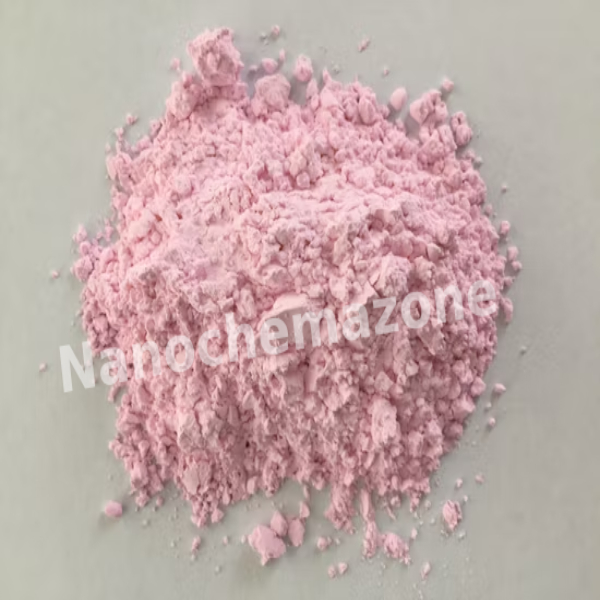
Erbium (III) Oxide (Er2O3) 99.99% 4N Powder

Price range: $293.00 through $1,943.00
Select options This product has multiple variants. The options may be chosen on the product page
Product Erbium (III) Oxide (Er2O3) 99.99% 4N Powder
CAS No. 12061-16-4
Appearance Fine pink powder or crystalline
Purity ≥99%,  ≥99.9%,  ≥95%(Other purities are also available)
APS 20–30nm (Size Can be customized),  Ask for other available size range.
Ingredient Er2O3
Molecular Weight 372.998 g/mol
Melting Point 2,344 °C
Boiling Point 3,290 °C
Density 8.64 g/cm³
Product Codes NCZ-339I
 

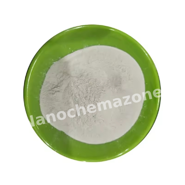
Hexagonal Boron Nitride (h-BN) Powder, 99% Purity, 1~2 um

Price range: $293.00 through $755.00
Select options This product has multiple variants. The options may be chosen on the product page
Product Hexagonal Boron Nitride (h-BN) Powder, 99% Purity, 1~2 um
CAS No. 10043-11-5
Appearance White to off-white
Purity ≥99%,  ≥99.9%,  ≥95%(Other purities are also available)
APS 1–2µm (Size Can be customized),  Ask for other available size range.
Ingredient BN
Molecular Weight 24.82 g/mol
Melting Point N/A
Boiling Point N/A
Density 2.1 g/cm³
Product Codes NCZ-373I

Ytterbium Oxide (Yb2O3) Nanoparticles, 40nm, >99.9% Purity, 25g

$293.00
Product Ytterbium Oxide (Yb2O3) Nanoparticles, 40nm, >99.9% Purity, 25g
CAS No. 1314-37-0
Appearance White
Purity ≥99%,  ≥99.9%,  ≥95%(Other purities are also available)
APS 40nm (Size Can be customized),  Ask for other available size range.
Ingredient Yb2O3
Molecular Weight 394.08 g/mol
Melting Point N/A
Boiling Point N/A
Density 9.17 g/cm³
Product Codes NCZ-598I
 

Bismuth (Bi) Sputtering Targets, Purity: 99.999%, Size: 2”, Thickness: 0.125”

$293.00

Product 

Bismuth (Bi) Sputtering Targets, Purity: 99.999%, Size: 2'', Thickness: 0.125''

CAS No.

7440‑69‑9

Appearance

Powder

Purity

≥99%,  ≥99.9%,  ≥95%

(Other purities are also available)

APS

1 – 5 µm (Size Can be customized), Ask for other available size ranges.

Ingredient

N/A

Molecular Weight

~208.98 g/mol

Melting Point

 271.4 °C

Boiling Point

~1560 °C

Density

 ~9.78–9.80 g/cm³

Product Codes

NCZ-2438K

Aluminum Oxide (Al2O3) Sputtering Targets, Purity: 99.99%, Size: 1”, Thickness: 0.250”

$293.00

Product 

Aluminum Oxide (Al2O3) Sputtering Targets, Purity: 99.99%, Size: 1'', Thickness: 0.250''

CAS No.

 1344-28-1

Appearance

Powder

Purity

≥99%,  ≥99.9%,  ≥95%

(Other purities are also available)

APS

N/A (Size Can be customized), Ask for other available size ranges.

Ingredient

N/A

Molecular Weight

101.96 g/mol

Melting Point

~2,072 °C

Boiling Point

~2,977 °C

Density

~3.97–3.98 g/cm³

Product Codes

NCZ-2548K

Aluminum (Al) Sputtering Targets, Purity: 99.999%, Size: 8”, Thickness: 0.125”

$293.00

Product 

Aluminum (Al) Sputtering Targets, Purity: 99.999%, Size: 8'', Thickness: 0.125''

CAS No.

 7429-90-5

Appearance

Powder

Purity

≥99%,  ≥99.9%,  ≥95%

(Other purities are also available)

APS

N/A (Size Can be customized), Ask for other available size ranges.

Ingredient

N/A

Molecular Weight

 26.98 g/mol

Melting Point

 660.3 °C

Boiling Point

 2519 °C

Density

 2.70 g/cm³

Product Codes

NCZ-2564K