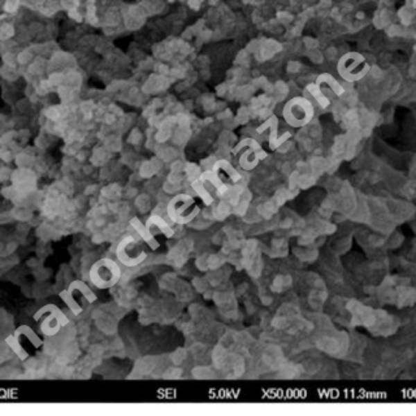
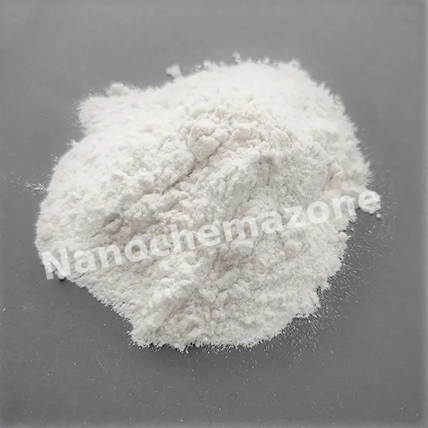
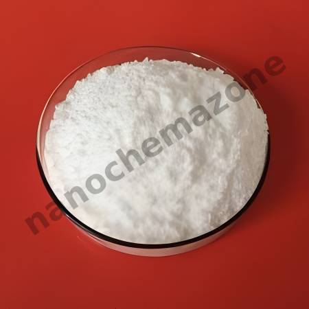
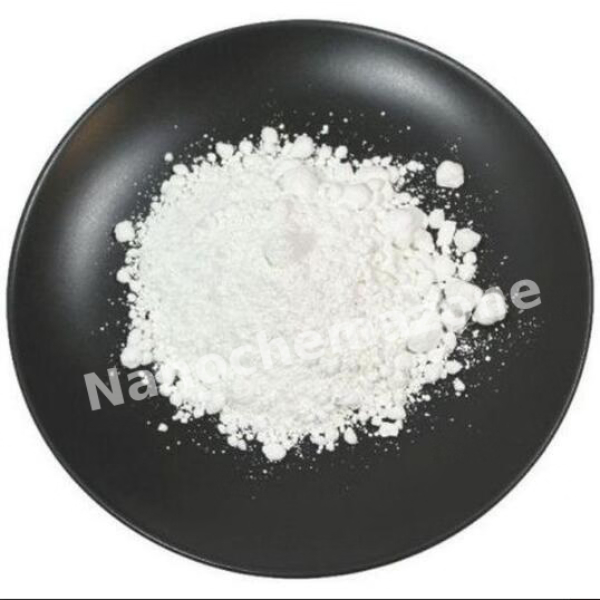
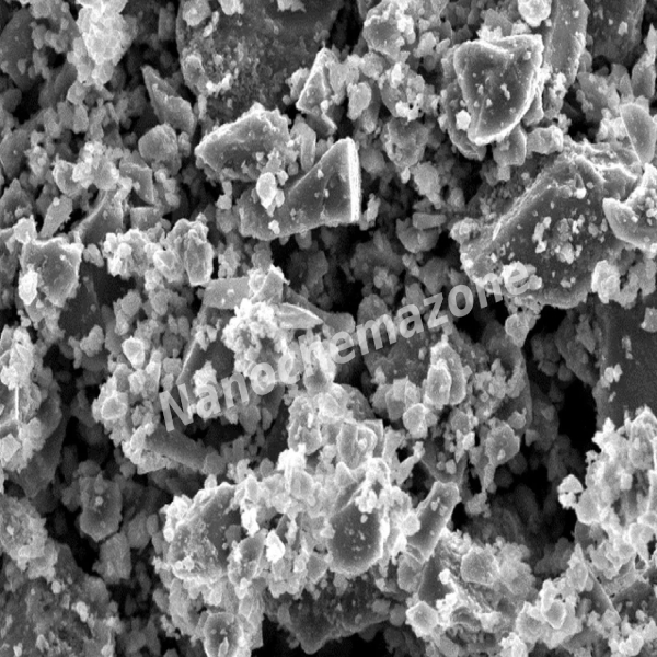
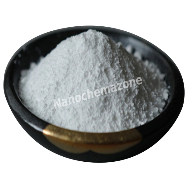
Hydroxyapatite(Ca10(PO4)6(OH)2, Medical grade, >98%, <10μm) (211982)

$275.00
Select options This product has multiple variants. The options may be chosen on the product page

Product 

Hydroxyapatite(Ca10(PO4)6(OH)2, Medical grade, >98%, <10μm) (211982)

CAS No.

1306‑06‑5

Appearance

Powder

Purity

≥99%,  ≥99.9%,  ≥95%

(Other purities are also available)

APS

 <10 µm (Size Can be customized), Ask for other available size ranges.

Ingredient

N/A

Molecular Weight

~1004.7 g/mo

Melting Point

~1670 °C

Boiling Point

N/A

Density

 ~3.16 g/cm³ (calculated) to 3.18 g/cm³ (literature)

Product Codes

NCZ-2602K

Strong Graphene Aerogel, Diameter: 2±0.4 cm, Height: 2±0.4 cm

Price range: $276.00 through $1,109.00
Select options This product has multiple variants. The options may be chosen on the product page
Please contact us for quotes for larger quantities !   Graphene aerogels are materials which have elasticity and they can easily gain their original form after some compression. In addition, the low density of graphene aerogels enables them to be very absorbent. This material can absorb more than 850 times of its own weight. This property means that it could be useful for environmental clean-ups like oil spills, and the aerogels only need to be picked up later after absorbing the spilled material. Graphene aerogel may also have some applications in both the storage and the transfer of energy by enabling the creation of lighter, higher-energy-density batteries and vigorous research is being done on the matter.

Multi Walled Carbon Nanotubes Ethanol Dispersion, 4 wt%, Purity: > 96%, OD: 3-13 nm, Length: 45 µm

Price range: $276.00 through $1,268.00
Select options This product has multiple variants. The options may be chosen on the product page
15 ml/251 € 30 ml/410 € 60 ml/710 € 120 ml/1150 € Please contact us for quotes on larger quantities !!!

Multi Walled Carbon Nanotubes Ethanol Dispersion

4 wt%, Purity: > 96+ %, OD: 3-13 nm, Length: 45 µm

Technical Properties:

Purity > 96+ %
Color black
Average Outside Diameter (nm) 3-13
Average Inside Diameter (nm) 3.0-5.0
Length (µm) 45
Tap Density (g/cm3) 0.30
True Density (g/cm3) 2.4
Specific Surface Area (m2/g) 240
Ash < 1.5 wt%
Electrical Conductivity (S/cm) > 98
Manufacturing Method CVD

Applications:

MWCNTs have a variety of potential applications in different fields. These applications include medicine, mechanical, electric, chemical, energy and others. It can be applied in, 1-drug delivery, 2-biosensors, 3-CNT composites, 4-catalysis, 5-nanoprobes, 6-hydrogen storage, 7-lithium batteries, 8-gas-discharge tubes, 9-flat panel display, 10-supercapacitor, 11-transistors, 12-solar cells, 13-photoluminescence, 14-template  

Magnesium (Mg) Sputtering Targets, Purity: 99.98%, Size: 5”, Thickness: 0.125”

$276.00

Applications of Sputtering Targets;

Film deposition is accomplished using sputtering targets. A technique for sputtering thin films is called "deposition made by sputter targets," which entails eroding material from a "target" source onto a "substrate" like a silicon wafer. Etching of the target is done using semiconductor sputtering targets. When selectivity is not an issue and a high degree of etching anisotropy is required, sputter etching is the method of choice. By removing the target material through etching, sputter targets are also utilized for investigation. In secondary ion spectroscopy (SIMS), one example is when the target material is sputtered at a steady pace. Mass spectrometry is used to quantify the concentration and identity of spewed atoms as the target is sputtered.

The target material's composition may be ascertained and even very low concentrations of contaminants can be found with the aid of the sputtering target.

There is also an application area for sputtering targets in space. One type of space weathering that alters the chemical and physical characteristics of airless worlds like the Moon and asteroids is sputtering.

Tungsten (W) Sputtering Targets, Purity: 99.95%, Size: 2”, Thickness: 0.250”

$276.00

Applications of Sputtering Targets;

Film deposition is accomplished using sputtering targets. A technique for sputtering thin films is called "deposition made by sputter targets," which entails eroding material from a "target" source onto a "substrate" like a silicon wafer. Etching of the target is done using semiconductor sputtering targets. When selectivity is not an issue and a high degree of etching anisotropy is required, sputter etching is the method of choice. By removing the target material through etching, sputter targets are also utilized for investigation. In secondary ion spectroscopy (SIMS), one example is when the target material is sputtered at a steady pace. Mass spectrometry is used to quantify the concentration and identity of spewed atoms as the target is sputtered.

The target material's composition may be ascertained and even very low concentrations of contaminants can be found with the aid of the sputtering target.

There is also an application area for sputtering targets in space. One type of space weathering that alters the chemical and physical characteristics of airless worlds like the Moon and asteroids is sputtering.

Zinc (Zn) Sputtering Targets, Purity: 99.95%, Size: 8”, Thickness: 0.250”

$276.00

Applications of Sputtering Targets;

Film deposition is accomplished using sputtering targets. A technique for sputtering thin films is called "deposition made by sputter targets," which entails eroding material from a "target" source onto a "substrate" like a silicon wafer. Etching of the target is done using semiconductor sputtering targets. When selectivity is not an issue and a high degree of etching anisotropy is required, sputter etching is the method of choice. By removing the target material through etching, sputter targets are also utilized for investigation. In secondary ion spectroscopy (SIMS), one example is when the target material is sputtered at a steady pace. Mass spectrometry is used to quantify the concentration and identity of spewed atoms as the target is sputtered.

The target material's composition may be ascertained and even very low concentrations of contaminants can be found with the aid of the sputtering target.

There is also an application area for sputtering targets in space. One type of space weathering that alters the chemical and physical characteristics of airless worlds like the Moon and asteroids is sputtering.

3N5 (99.95%) Niobium Oxide (Nb2O5) Pieces (3-12mm) Evaporation Materials

Price range: $276.00 through $628.00
Select options This product has multiple variants. The options may be chosen on the product page
Product 3N5 (99.95%) Niobium Oxide (Nb2O5) Pieces (3-12mm) Evaporation Materials
CAS No. 1313-96-8
Appearance White, Crystalline Solid, Grey-Black
Purity ≥99%,  ≥99.9%,  ≥95%(Other purities are also available)
APS 3-12mm (Size Can be customized),  Ask for other available size range.
Ingredient Nb2O5
Molecular Weight 265.81 g/mol
Melting Point 1,485 °C
Boiling Point N/A
Density 4.6 g/cm3
Product Codes NCZ-145E
 

Titanium Dioxide (TiO2) Sputtering Targets, Purity: 99.9%, Size: 1”, Thickness: 0.125”, Grey to Black

$276.00

Product 

Titanium Dioxide (TiO2) Sputtering Targets, Purity: 99.9%, Size: 1'', Thickness: 0.125'', Grey to Black

CAS No.

13463‑67‑7

Appearance

Powder

Purity

≥99%,  ≥99.9%,  ≥95%

(Other purities are also available)

APS

TiO₂ (black granules) (Size Can be customized), Ask for other available size ranges.

Ingredient

N/A

Molecular Weight

79.94 g/mol

Melting Point

~1,843 °C

Boiling Point

~2,972 °C

Density

~4.23 g/cm³

Product Codes

NCZ-1445K

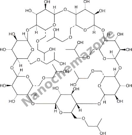
Hydroxypropyl β-Cyclodextrin (242605)

$276.00
Select options This product has multiple variants. The options may be chosen on the product page
Hydroxypropyl β-Cyclodextrin (242605)

Feature:
Hydroxypropyl beta-Cyclodextrin are purified polydisperse products resulting from the controlled reaction of propylene oxide and native beta-cyclodextrin. Hydroxypropyl beta-cyclodextrin is itself very soluble in water (greater than 500 mg/ml at room temperature compared to 18 mg/ml for beta-cyclodextrin), and is used for molecular encapsulation of a variety of sparingly water compounds to enhance the aqueous solubility of the encapsulated compound. CAS : 128446-35-5 Molecular Formula: C63H112O42

Molecular Weight:  1541.54

 Specifications:

1. Appearance: White powder

2. Assay: ≥98%

3. Loss on Drying: ≤4.5%

4. Chloride: ≤0.02%

5. Residue on Ignition: ≤1.5%

6. Heavy Metals: ≤0.0025%

7. As: ≤0.0002%

8. Degree of substitution: 4-9

9. Total bacteria count: ≤1000 pcs/g

10. Moulds and yeasts: ≤100 pcs/g

Product Codes- NCZ-2763K

Monolayer Graphene on SiO2/Si Substrate, Size: 2″

Price range: $277.00 through $1,126.00
Select options This product has multiple variants. The options may be chosen on the product page

Applications:

Graphene research; Supercapacitors; Catalyst; Solar energy; Graphene optoelectronics, plasmonics and nanophotonics; Graphene semiconductor chips; Conductive graphene film; Graphene computer memory; Biomaterials and Bioelectronics

Multi Walled Carbon Nanotubes Ethanol Dispersion, 4 wt%, Purity: > 96 %, OD: 45-75 nm,Length 8-28 µm

Price range: $277.00 through $1,268.00
Select options This product has multiple variants. The options may be chosen on the product page
15 ml/252 € 30 ml/420 €  60 ml/720 € 120 ml/1150 €  
Please contact us for quotes on larger quantities !!!

Multi Walled Carbon Nanotubes Ethanol Dispersion

4 wt%, Purity: > 96+ %, OD: 45-75 nm, Length 8-28 µm

Technical Properties:

Purity > 96+ %
Color black
Average Outside Diameter (nm) 45-75
Average Inside Diameter (nm) 5.0-10.0
Length (μm) 8-28
Tap Density (g/cm3) 0.30
True Density (g/cm3) 2.4
Specific Surface Area (m2/g) 50
Ash < 1.5 wt%
Electrical Conductivity (S/cm) > 98
Manufacturing Method CVD

Applications:

MWCNTs have a variety of potential applications in different fields. These applications include midicine, mechanical, electric, chemical, energy and others. It can be applied in, 1-drug dilevery, 2-biosensors, 3-CNT composites, 4-catalysis, 5-nanoprobes, 6-hydrogen storage, 7-lithium battaries, 8-gas-discharge tubes, 9-flat panel display, 10-supercapacitor, 11-transistors, 12-solar cells, 13-photoluminescence, 14-template  

Multi Walled Carbon Nanotubes Isopropanol Dispersion, 4 wt%, Purity: > 95%, OD: 18-35 nm, Length: 8-18 µm

Price range: $277.00 through $1,229.00
Select options This product has multiple variants. The options may be chosen on the product page
15 ml/252 € 30 ml/420 € 60 ml/725 € 120 ml/1115 €
Please contact us for quotes on larger quantities !!!

Multi Walled Carbon Nanotubes Isopropanol Dispersion

4 wt%, Purity: > 95+ %, OD: 18-35 nm, Length: 8-18 µm

Technical Properties:

Purity > 95+ %
Color black
Average Outside Diameter (nm) 18-35
Average Inside Diameter (nm) 5.0-10.0
Length (μm) 8-18
Tap Density (g/cm3) 0.30
True Density (g/cm3) 2.4
Specific Surface Area (m2/g) 120
Ash < 1.5 wt%
Electrical Conductivity (S/cm) > 98
Manufacturing Method CVD

Applications:

MWCNTs have a variety of potential applications in different fields. These applications include midicine, mechanical, electric, chemical, energy and others. It can be applied in, 1-drug dilevery, 2-biosensors, 3-CNT composites, 4-catalysis, 5-nanoprobes, 6-hydrogen storage, 7-lithium battaries, 8-gas-discharge tubes, 9-flat panel display, 10-supercapacitor, 11-transistors, 12-solar cells, 13-photoluminescence, 14-template  

Multi Walled Carbon Nanotubes Isopropanol Dispersion, 4wt%, Purity: > 96%, OD: 4-12 nm, Length: 55 µm

Price range: $277.00 through $1,191.00
Select options This product has multiple variants. The options may be chosen on the product page
15 ml/252 € 30 ml/420 € 60 ml/706 € 120 ml/1080 €   
Please contact us for quotes on larger quantities !!!

Multi Walled Carbon Nanotubes Isopropanol Dispersion

4 wt%, Purity: > 96+ %, OD: 4-12 nm, Length: 55 µm

Technical Properties:

Purity > 96+ %
Color black
Average Outside Diameter (nm) 4-12
Average Inside Diameter (nm) 3.0-5.0
Length (µm) 55
Tap Density (g/cm3) 0.30
True Density (g/cm3) 2.4
Specific Surface Area (m2/g) 240
Ash < 1.5 wt%
Electrical Conductivity (S/cm) > 98
Manufacturing Method CVD

Applications:

MWCNTs have a variety of potential applications in different fields. These applications include medicine, mechanical, electric, chemical, energy and others. It can be applied in, 1-drug delivery, 2-biosensors, 3-CNT composites, 4-catalysis, 5-nanoprobes, 6-hydrogen storage, 7-lithium batteries, 8-gas-discharge tubes, 9-flat panel display, 10-supercapacitor, 11-transistors, 12-solar cells, 13-photoluminescence, 14-template

Yttrium (Y) Sputtering Targets, Purity: 99.9%, Size: 1”, Thickness: 0.250”

$277.00

Applications of Sputtering Targets;

  • Sputtering targets is used for film deposition. The deposition made by sputter targets is a method of depositing thin films by sputtering that involves eroding material from a "target" source onto a "substrate" such as  a silicon wafer.
  • Semiconductor sputtering targets is used to etch the target. Sputter etching is chosen in cases where a high degree of etching anisotropy is needed and selectivity is not a concern.
  • Sputter targets is also used for analysis by etching away the target material.
One of the example occurs in secondary ion spectroscopy (SIMS), where the target sample is sputtered at a constant rate. As the target is sputtered, the concentration and identity of sputtered atoms are measured using mass spectrometry. By helping of the sputtering target, the composition of the target material can be determined and even extremely low concentrations of impurities are detected. Sputtering target has also application area in space. Sputtering is one of the forms of space weathering, a process that changes the physical and chemical properties of airless bodies, such as asteroids and the Moon.

Nickel (Ni) Sputtering Targets, Purity: 99.995%, Size: 4”, Thickness: 0.125”

$277.00

Applications of Sputtering Targets;

Film deposition is accomplished using sputtering targets. A technique for sputtering thin films is called "deposition made by sputter targets," which entails eroding material from a "target" source onto a "substrate" like a silicon wafer. Etching of the target is done using semiconductor sputtering targets. When selectivity is not an issue and a high degree of etching anisotropy is required, sputter etching is the method of choice. By removing the target material through etching, sputter targets are also utilized for investigation. In secondary ion spectroscopy (SIMS), one example is when the target material is sputtered at a steady pace. Mass spectrometry is used to quantify the concentration and identity of spewed atoms as the target is sputtered.

By helping of the sputtering target, the composition of the target material may be evaluated and even extremely tiny amounts of contaminants are recognized.

There is also an application area for sputtering targets in space. One type of space weathering that alters the chemical and physical characteristics of airless worlds like the Moon and asteroids is sputtering.

Calcium phytate (339604)

$277.00
Select options This product has multiple variants. The options may be chosen on the product page
Calcium phytate (339604)
preduct name Cutcium pbgtate
Chemical nume Inesit"l Hexopbøsphøric Cutcium Salt
M"leculor førmula C6H6024P6C06
CAS 361 5-82-5
Appl i catiøn White pewder. Calcium phgtote is kind "f drug moteriols with wide range "f appl icotiøn. It can speed up the metastasis "f human b"dg, keep the pbøspb"rus balance "f humun b"dg, nøurisb the bruin etc.. Mainly used in tbe fields including grease, pharmaceutical und feedstuffs etc..
Specificatien S ecificdtiøn
Index name Index
Centent 9870min
physpbmus 20.2-21.8%
Calcium 26.4 Zmin
Arsenic 3ppm max
Heavg metal 1 5ppm max
Løss "n drging 201mc1/
Pesidue "n ignitiøn 70-801
Støroge Kept awog fro") light "r heat.
Product Codes- NCZ-2626K

Boron Oxide (B2O3) Nanopowder/Nanoparticles, Purity: 99.95 %, Size: 50 nm

Price range: $278.00 through $3,957.00
Select options This product has multiple variants. The options may be chosen on the product page
25 grams/245 €                       
100 grams/490 €                     
500 grams/1960 €                    
1000 grams/3480 €
Please contact us for quotes on larger quantities !!!              

Boron Oxide (B2O3) Nanopowder/Nanoparticles

Purity: 99.95 %, Size: 50 nm

Multi Walled Carbon Nanotubes Ethanol Dispersion, 4 wt%, Purity: > 96 %, OD: 45-75 nm,Length 8-28 µm

Price range: $278.00 through $1,265.00
Select options This product has multiple variants. The options may be chosen on the product page
Multi Walled Carbon Nanotubes Ethanol Dispersion 4 wt%, Purity: > 96+ %, OD: 45-75 nm, Length 8-28 µm Technical Properties: Purity

Silver Nanowire Dispersion

Price range: $279.00 through $567.00
Select options This product has multiple variants. The options may be chosen on the product page
Product Silver Nanowire Dispersion
CAS No. 7440-22-4
Appearance Transparent to slightly cloudy liquid
Purity ≥99%,  ≥99.9%,  ≥95%(Other purities are also available)
APS 5–100µm (Size Can be customized),  Ask for other available size range.
Ingredient Ag
Molecular Weight N/A
Melting Point N/A
Boiling Point N/A
Density N/A
Product Codes NCZ-523I

Lithium Titanate (Li2TiO3) Sputtering Targets, indium, Purity: 99.95%, Size: 2”, Thickness: 0.125”

$280.00

Applications of Sputtering Targets;

Film deposition is accomplished using sputtering targets. A technique for sputtering thin films is called "deposition made by sputter targets," which entails eroding material from a "target" source onto a "substrate" like a silicon wafer. Etching of the target is done using semiconductor sputtering targets. When selectivity is not an issue and a high degree of etching anisotropy is required, sputter etching is the method of choice. By removing the target material through etching, sputter targets are also utilized for investigation. In secondary ion spectroscopy (SIMS), one example is when the target material is sputtered at a steady pace. Mass spectrometry is used to quantify the concentration and identity of spewed atoms as the target is sputtered.

By helping of the sputtering target, the composition of the target material may be evaluated and even extremely tiny amounts of contaminants are recognized.

There is also an application area for sputtering targets in space. One type of space weathering that alters the chemical and physical characteristics of airless worlds like the Moon and asteroids is sputtering.

Magnesium (Mg) Sputtering Targets, Purity: 99.98%, Size: 4”, Thickness: 0.250”

$280.00

Product 

Magnesium (Mg) Sputtering Targets, Purity: 99.98%, Size: 4'', Thickness: 0.250''

CAS No.

7439-95-4

Appearance

Powder

Purity

≥99%,  ≥99.9%,  ≥95%

(Other purities are also available)

APS

 N/A (Size Can be customized), Ask for other available size ranges.

Ingredient

N/A

Molecular Weight

 24.305 g/mol

Melting Point

 650 °C

Boiling Point

 1,090 °C

Density

1.738 g/cm³

Product Codes

NCZ-1992K

Lanthanum (III) Oxide (La2O3) 99.9995% 5N5 High Purity Powder

$280.00
Select options This product has multiple variants. The options may be chosen on the product page
Product Lanthanum (III) Oxide (La2O3) 99.9995% 5N5 High Purity Powder
CAS No. 12037-29-5
Appearance White to off-white
Purity ≥99%,  ≥99.9%,  ≥95%(Other purities are also available)
APS 1–10nm (Size Can be customized),  Ask for other available size range.
Ingredient La2O3
Molecular Weight 325.81 g/mol
Melting Point 2,230 °C
Boiling Point N/A
Density 6.51 g/cm³
Product Codes NCZ-435I

Sodium phytate(from rice, Daily chemical industry Grade) (338604)

$280.00
Select options This product has multiple variants. The options may be chosen on the product page

Product 

Sodium phytate(from rice, Daily chemical industry Grade) (338604)

CAS No.

14306‑25‑3

Appearance

Powder

Purity

≥99%,  ≥99.9%,  ≥95%

(Other purities are also available)

APS

  10–500 µm (Size Can be customized), Ask for other available size ranges.

Ingredient

N/A

Molecular Weight

 684.03 g/mol

Melting Point

 53.3–53.9 °C

Boiling Point

N/A

Density

 2.04 g/cm³ at 20 °C

Product Codes

NCZ-2618K

Copper(II) sulfide(CuS·H2O, 97%) (302642)

$280.00
Select options This product has multiple variants. The options may be chosen on the product page
Copper(II) sulfide(CuS·H2O, 97%) (302642)

 
Product Codes- NCZ-2747K

Carbon Nanotubes(CNT) Modified Graphene Aerogel, Diameter: 2±0.4 cm, Height: 2±0.4 cm

Price range: $281.00 through $1,123.00
Select options This product has multiple variants. The options may be chosen on the product page
Please contact us for quotes for larger quantities !   Graphene aerogels are materials which have elasticity and they can easily gain their original form after some compression. In addition, the low density of graphene aerogels enables them to be very absorbent. This material can absorb more than 850 times of its own weight. This property means that it could be useful for environmental clean-ups like oil spills, and the aerogels only need to be picked up later after absorbing the spilled material. Graphene aerogel may also have some applications in both the storage and the transfer of energy by enabling the creation of lighter, higher-energy-density batteries and vigorous research is being done on the matter.

Nickel Vanadium (NiV) Sputtering Targets, Purity: 99.95%, Size: 2”, Thickness: 0.250”

$281.00

Product 

Nickel Vanadium (NiV) Sputtering Targets, Purity: 99.95%, Size: 2'', Thickness: 0.250''

CAS No.

11137-91-4

Appearance

Powder

Purity

≥99%,  ≥99.9%,  ≥95%

(Other purities are also available)

APS

N/A (Size Can be customized), Ask for other available size ranges.

Ingredient

N/A

Molecular Weight

~57.9 g/mol

Melting Point

~1,350–1,450 °C

Boiling Point

N/A

Density

 ~8.5 g/cm³

Product Codes

NCZ-1827K

Barium Carbonate (BaCO3) 99.999% 5N High Purity Powder

$281.00
Select options This product has multiple variants. The options may be chosen on the product page
Product Barium Carbonate (BaCO3) 99.999% 5N High Purity Powder
CAS No. 513-77-9
Appearance White or crystalline granules
Purity ≥99%,  ≥99.9%,  ≥95%(Other purities are also available)
APS 40–60µm (Size Can be customized),  Ask for other available size range.
Ingredient BaCO3
Molecular Weight 197.34 g/mol
Melting Point N/A
Boiling Point N/A
Density 4.286 g/cm³
Product Codes NCZ-294I

Nickel Chromium (Ni-Cr) Sputtering Targets, Purity: 99.9%, Size: 3”, Thickness: 0.125”

$282.00

Applications of Sputtering Targets;

Film deposition is accomplished using sputtering targets. A technique for sputtering thin films is called "deposition made by sputter targets," which entails eroding material from a "target" source onto a "substrate" like a silicon wafer. Etching of the target is done using semiconductor sputtering targets. When selectivity is not an issue and a high degree of etching anisotropy is required, sputter etching is the method of choice. By removing the target material through etching, sputter targets are also utilized for investigation. In secondary ion spectroscopy (SIMS), one example is when the target material is sputtered at a steady pace. Mass spectrometry is used to quantify the concentration and identity of spewed atoms as the target is sputtered.

The target material's composition may be ascertained and even very low concentrations of contaminants can be found with the aid of the sputtering target.

There is also an application area for sputtering targets in space. One type of space weathering that alters the chemical and physical characteristics of airless worlds like the Moon and asteroids is sputtering.

Silicon Nitride (Si3N4) Sputtering Targets, Purity: 99.9%, Size: 1”, Thickness: 0.250”, White to Gray

$282.00

Applications of Sputtering Targets;

Film deposition is accomplished using sputtering targets. A technique for sputtering thin films is called "deposition made by sputter targets," which entails eroding material from a "target" source onto a "substrate" like a silicon wafer. Etching of the target is done using semiconductor sputtering targets. When selectivity is not an issue and a high degree of etching anisotropy is required, sputter etching is the method of choice. By removing the target material through etching, sputter targets are also utilized for investigation. In secondary ion spectroscopy (SIMS), one example is w

The target material's composition may be ascertained and even very low concentrations of contaminants can be found with the aid of the sputtering target.

There is also an application area for sputtering targets in space. One type of space weathering that alters the chemical and physical characteristics of airless worlds like the Moon and asteroids is sputtering.

hen the target material is sputtered at a steady pace. Mass spectrometry is used to quantify the concentration and identity of spewed atoms as the target is sputtered.

Titanium Dioxide (TiO2) Sputtering Targets, Purity: 99.9%, Size: 1”, Thickness: 0.250”, Grey to Black

$282.00

Applications of Sputtering Targets;

Film deposition is accomplished using sputtering targets. A technique for sputtering thin films is called "deposition made by sputter targets," which entails eroding material from a "target" source onto a "substrate" like a silicon wafer. Etching of the target is done using semiconductor sputtering targets. When selectivity is not an issue and a high degree of etching anisotropy is required, sputter etching is the method of choice. By removing the target material through etching, sputter targets are also utilized for investigation. In secondary ion spectroscopy (SIMS), one example is when the target material is sputtered at a steady pace. Mass spectrometry is used to quantify the concentration and identity of spewed atoms as the target is sputtered.

The target material's composition may be ascertained and even very low concentrations of contaminants can be found with the aid of the sputtering target.

There is also an application area for sputtering targets in space. One type of space weathering that alters the chemical and physical characteristics of airless worlds like the Moon and asteroids is sputtering.

Vanadium (V) Sputtering Targets, Purity: 99.5%, Size: 2”, Thickness: 0.250”

$282.00

Applications of Sputtering Targets;

Film deposition is accomplished using sputtering targets. A technique for sputtering thin films is called "deposition made by sputter targets," which entails eroding material from a "target" source onto a "substrate" like a silicon wafer. Etching of the target is done using semiconductor sputtering targets. When selectivity is not an issue and a high degree of etching anisotropy is required, sputter etching is the method of choice. By removing the target material through etching, sputter targets are also utilized for investigation. In secondary ion spectroscopy (SIMS), one example is when the target material is sputtered at a steady pace. Mass spectrometry is used to quantify the concentration and identity of spewed atoms as the target is sputtered.

Nickel (Ni) Sputtering Targets, Purity: 99.99%, Size: 4”, Thickness: 0.250”

$283.00

Product 

Nickel (Ni) Sputtering Targets, Purity: 99.99%, Size: 4'', Thickness: 0.250''

CAS No.

7440-02-0

Appearance

Powder

Purity

≥99%,  ≥99.9%,  ≥95%

(Other purities are also available)

APS

 N/A (Size Can be customized), Ask for other available size ranges.

Ingredient

N/A

Molecular Weight

 58.69 g/mol

Melting Point

 1,455 °C

Boiling Point

 2,732 °C

Density

 8.90 g/cm³

Product Codes

NCZ-1876K

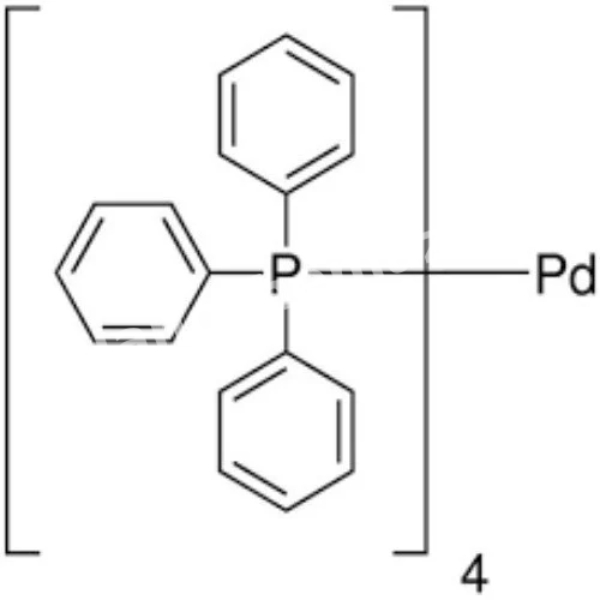
Tetrakis(triphenylphosphine)palladium, Pd(PPh3)4, >98%

Price range: $283.00 through $2,189.00
Select options This product has multiple variants. The options may be chosen on the product page
Product Tetrakis(triphenylphosphine)palladium, Pd(PPh3)4, >98%
CAS No. 14221-01-3
Appearance Yellow crystalline
Purity ≥99%,  ≥99.9%,  ≥95%(Other purities are also available)
APS 10–100µm (Size Can be customized),  Ask for other available size range.
Ingredient Pd(PPh₃)₄
Molecular Weight 1155.52 g/mol
Melting Point 121–123 °C
Boiling Point N/A
Density 7.3 g/cm³
Product Codes NCZ-553I
 

Bismuth (Bi) Sputtering Target

Price range: $284.00 through $762.00
Select options This product has multiple variants. The options may be chosen on the product page

Product 

Bismuth (Bi) Sputtering Target

CAS No.

7440-69-9

Appearance

Powder

Purity

≥99%,  ≥99.9%,  ≥95%

(Other purities are also available)

APS

 NA (Size Can be customized), Ask for other available size ranges.

Ingredient

N/A

Molecular Weight

208.98 g/mol

Melting Point

271.4 °C

Boiling Point

 1,560 °C

Density

9.78 g/cm³

Product Codes

NCZ-1347K

Cerium (Ce) Sputtering Target

Price range: $284.00 through $762.00
Select options This product has multiple variants. The options may be chosen on the product page

Product 

Cerium (Ce) Sputtering Target

CAS No.

7440-45-1

Appearance

Powder

Purity

≥99%,  ≥99.9%,  ≥95%

(Other purities are also available)

APS

 NA (Size Can be customized), Ask for other available size ranges.

Ingredient

N/A

Molecular Weight

140.12 g/mol

Melting Point

798 °C

Boiling Point

3,426 °C

Density

6.77 g/cm³

Product Codes

NCZ-1350K

Erbium (Er) Sputtering Target

Price range: $284.00 through $762.00
Select options This product has multiple variants. The options may be chosen on the product page

Product 

Erbium (Er) Sputtering Target

CAS No.

 7429-91-6

Appearance

Powder

Purity

≥99%,  ≥99.9%,  ≥95%

(Other purities are also available)

APS

 NA (Size Can be customized), Ask for other available size ranges.

Ingredient

N/A

Molecular Weight

162.5 g/mol

Melting Point

1,407 °C

Boiling Point

2,567 °C

Density

8.55 g/cm³

Product Codes

NCZ-1354K

Strontium (Sr) Sputtering Target

Price range: $284.00 through $762.00
Select options This product has multiple variants. The options may be chosen on the product page

Product 

Strontium (Sr) Sputtering Target

CAS No.

7440-24-6

Appearance

Powder

Purity

≥99%,  ≥99.9%,  ≥95%

(Other purities are also available)

APS

 NA (Size Can be customized), Ask for other available size ranges.

Ingredient

N/A

Molecular Weight

87.62 g/mol

Melting Point

777 °C

Boiling Point

 1,382 °C

Density

 2.64 g/cm³

Product Codes

NCZ-1360K

Yttrium (Y) Sputtering Target

Price range: $284.00 through $762.00
Select options This product has multiple variants. The options may be chosen on the product page

Product 

Yttrium (Y) Sputtering Target

CAS No.

7440-65-5

Appearance

Powder

Purity

≥99%,  ≥99.9%,  ≥95%

(Other purities are also available)

APS

 NA (Size Can be customized), Ask for other available size ranges.

Ingredient

N/A

Molecular Weight

88.91 g/mol

Melting Point

 1,522 °C

Boiling Point

 3,345 °C

Density

 4.47 g/cm³

Product Codes

NCZ-1364K

Bismuth Oxide (Bi2O3) Sputtering Target

Price range: $284.00 through $762.00
Select options This product has multiple variants. The options may be chosen on the product page

Product 

Bismuth Oxide (Bi2O3) Sputtering Target

CAS No.

1304-76-3

Appearance

Powder

Purity

≥99%,  ≥99.9%,  ≥95%

(Other purities are also available)

APS

 NA (Size Can be customized), Ask for other available size ranges.

Ingredient

N/A

Molecular Weight

465.96 g/mol

Melting Point

 817 °C

Boiling Point

~1,890 °C

Density

 8.9 – 9.3 g/cm³

Product Codes

NCZ-1366K

Chromium Oxide (Cr2O3) Sputtering Target

Price range: $284.00 through $762.00
Select options This product has multiple variants. The options may be chosen on the product page

Product 

Chromium Oxide (Cr2O3) Sputtering Target

CAS No.

 1308-38-9

Appearance

Powder

Purity

≥99%,  ≥99.9%,  ≥95%

(Other purities are also available)

APS

 NA (Size Can be customized), Ask for other available size ranges.

Ingredient

N/A

Molecular Weight

151.99 g/mol

Melting Point

2,435 °C

Boiling Point

N/A

Density

5.22 g/cm³

Product Codes

NCZ-1367K

Cobalt Oxide (CoO) Sputtering Target

Price range: $284.00 through $762.00
Select options This product has multiple variants. The options may be chosen on the product page

Product 

Cobalt Oxide (CoO) Sputtering Target

CAS No.

1307-96-6

Appearance

Powder

Purity

≥99%,  ≥99.9%,  ≥95%

(Other purities are also available)

APS

 NA (Size Can be customized), Ask for other available size ranges.

Ingredient

N/A

Molecular Weight

74.93 g/mol

Melting Point

1,935 °C

Boiling Point

Decomposes (~2,000 °C+)

Density

 6.45 g/cm³

Product Codes

NCZ-1368K

Lanthanum Oxide (La2O3) Sputtering Target

Price range: $284.00 through $762.00
Select options This product has multiple variants. The options may be chosen on the product page

Product 

Lanthanum Oxide (La2O3) Sputtering Target

CAS No.

1312-81-8

Appearance

Powder

Purity

≥99%,  ≥99.9%,  ≥95%

(Other purities are also available)

APS

 NA (Size Can be customized), Ask for other available size ranges.

Ingredient

N/A

Molecular Weight

 325.81 g/mol

Melting Point

2,313 °C

Boiling Point

~4,200 °C

Density

6.51 g/cm³

Product Codes

NCZ-1372K

Samarium Oxide (Sm2O3) Sputtering Target

Price range: $284.00 through $762.00
Select options This product has multiple variants. The options may be chosen on the product page

Product 

Samarium Oxide (Sm2O3) Sputtering Target

CAS No.

 12060‑58‑1

Appearance

Powder

Purity

≥99%,  ≥99.9%,  ≥95%

(Other purities are also available)

APS

 NA (Size Can be customized), Ask for other available size ranges.

Ingredient

N/A

Molecular Weight

~348.8 g/mol

Melting Point

~2,335 °C

Boiling Point

~4,118 °C

Density

 ~8.35 – 7.60 g/cm³

Product Codes

NCZ-1376K

Silicon Nitride (Si3N4) Sputtering Target

Price range: $284.00 through $762.00
Select options This product has multiple variants. The options may be chosen on the product page

Product 

Silicon Nitride (Si3N4) Sputtering Target

CAS No.

12033‑89‑5

Appearance

Powder

Purity

≥99%,  ≥99.9%,  ≥95%

(Other purities are also available)

APS

 NA (Size Can be customized), Ask for other available size ranges.

Ingredient

N/A

Molecular Weight

 140.28 g/mol

Melting Point

~1,900 °C

Boiling Point

N/A

Density

 ~2.2–3.5 g/cm³

Product Codes

NCZ-1382K

Silicon (Si) Sputtering Targets, N-type, Purity: 99.999%, Size: 1”, Thickness: 0.250”

$284.00

Product 

Silicon (Si) Sputtering Targets, N-type, Purity: 99.999%, Size: 1'', Thickness: 0.250''

CAS No.

7440-21-3

Appearance

Powder

Purity

≥99%,  ≥99.9%,  ≥95%

(Other purities are also available)

APS

N/A  (Size Can be customized), Ask for other available size ranges.

Ingredient

N/A

Molecular Weight

28.0855 g/mol

Melting Point

 1,414 °C

Boiling Point

3,265 °C

Density

 2.33 g/cm³

Product Codes

NCZ-1766K

Multi Walled Carbon Nanotubes Ethanol Dispersion, 4 wt%, Purity: > 96 %, OD: 45-75 nm,Length 8-28 µm

Price range: $285.00 through $1,301.00
Select options This product has multiple variants. The options may be chosen on the product page

Applications:

MWCNTs have a variety of potential applications in different fields. These applications include midicine, mechanical, electric, chemical, energy and others. It can be applied in, 1-drug dilevery, 2-biosensors, 3-CNT composites, 4-catalysis, 5-nanoprobes, 6-hydrogen storage, 7-lithium battaries, 8-gas-discharge tubes, 9-flat panel display, 10-supercapacitor, 11-transistors, 12-solar cells, 13-photoluminescence, 14-template

Holey Graphene

Price range: $285.00 through $1,380.00
Select options This product has multiple variants. The options may be chosen on the product page

Applications of Holey Graphene

Holey Super Graphene's exceptional properties — including ultra-high conductivity, expansive surface area, and superior electrochemical performance — position it as an adaptable material ideal for a broad spectrum of applications, from energy storage to environmental sensing. Its high conductivity will benefit energy storage by providing fast charge-discharge processes and long life advantages in battery and supercapacitor technologies. It will also find use in many different fields, from membranes to electronic devices, fuel cells to gas sensors, water treatment systems to hydrogen storage and biological research. You can find a summary list below.
  • Electronics: Enhances energy storage in supercapacitors and batteries due to its large surface area and ultra-high conductivity, leading to faster charge-discharge cycles and extended battery life.
  • Sensing Technology: Utilized in sensors for detecting gases and other molecular interactions, increasing sensitivity and response time in environmental monitoring and medical diagnostics.
  • Photonics and Optoelectronics: Applied in photodetectors and light-emitting devices, improving efficiency with its unique electronic and optical properties.
  • Clean Energy: Supports fuel cells and hydrogen storage, leveraging its high surface area to improve efficiency in energy conversion and storage, contributing to cleaner energy solutions.
  • Water Purification: Filters and purifies water at the nanoscale, enabling effective desalination and removal of impurities.
  • Environmental and Safety: Acts as a sensitive material in gas sensors for environmental monitoring and industrial safety, aiding in the detection of pollutants and hazardous gases.
  • Material Enhancement: Incorporated into nanocomposite materials to boost mechanical, electrical, and thermal properties for use in aerospace, automotive, and construction.

Calcium Manganate (CaMnO3) Sputtering Targets, Purity: 99.9%, Size: 1”, Thickness: 0.125”

$285.00

Applications of Sputtering Targets;

Film deposition is accomplished using sputtering targets. A technique for sputtering thin films is called "deposition made by sputter targets," which entails eroding material from a "target" source onto a "substrate" like a silicon wafer. Etching of the target is done using semiconductor sputtering targets. When selectivity is not an issue and a high degree of etching anisotropy is required, sputter etching is the method of choice. By removing the target material through etching, sputter targets are also utilized for investigation. In secondary ion spectroscopy (SIMS), one example is when the target material is sputtered at a steady pace. Mass spectrometry is used to quantify the concentration and identity of spewed atoms as the target is sputtered.

The target material's composition may be ascertained and even very low concentrations of contaminants can be found with the aid of the sputtering target.

There is also an application area for sputtering targets in space. One type of space weathering that alters the chemical and physical characteristics of airless worlds like the Moon and asteroids is sputtering.

Copper (Cu) Sputtering Targets, Purity: 99.999%, Size: 4”, Thickness: 0.125”

$285.00

Applications of Sputtering Targets;

Film deposition is accomplished using sputtering targets. A technique for sputtering thin films is called "deposition made by sputter targets," which entails eroding material from a "target" source onto a "substrate" like a silicon wafer. Etching of the target is done using semiconductor sputtering targets. When selectivity is not an issue and a high degree of etching anisotropy is required, sputter etching is the method of choice. By removing the target material through etching, sputter targets are also utilized for investigation. In secondary ion spectroscopy (SIMS), one example is when the target material is sputtered at a steady pace. Mass spectrometry is used to quantify the concentration and identity of spewed atoms as the target is sputtered.

The target material's composition may be ascertained and even very low concentrations of contaminants can be found with the aid of the sputtering target.

There is also an application area for sputtering targets in space. One type of space weathering that alters the chemical and physical characteristics of airless worlds like the Moon and asteroids is sputtering.

High Purity Graphene Water Dispersion (98%, 1~3nm)

Price range: $285.00 through $1,150.00
Select options This product has multiple variants. The options may be chosen on the product page
$285/1g $1150/5g
Product High Purity Graphene Water Dispersion (98%, 1~3nm)
CAS No. 7782-42-5
Appearance Dark grey to black powder
Purity ≥99%,  ≥99.9%,  ≥95%(Other purities are also available)
APS 10nm (Size Can be customized),  Ask for other available size range.
Ingredient C
Molecular Weight 12.01 g/mol
Melting Point 3697 °C
Boiling Point 4830 °C
Density N/A
Product Codes NCZ-106G
 

High Purity Graphene Aqueous Paste (98%, <10nm)
Price range: $285.00 through $1,285.00
Select options This product has multiple variants. The options may be chosen on the product page
$285/1g $1285/5g
Product High Purity Graphene Aqueous Paste (98%, <10nm)
CAS No. 7782-42-5
Appearance Aqueous paste powder
Purity ≥99%,  ≥99.9%,  ≥95%(Other purities are also available)
APS 10nm (Size Can be customized),  Ask for other available size range.
Ingredient C
Molecular Weight 12.01 g/mol
Melting Point 3697 °C
Boiling Point 4200 °C
Density N/A
Product Codes NCZ-107G
 

Ampcera Li-doped Sodium Beta Alumina Solid Electrolyte Powder, β”-Al2O3 + Li, 99.99% Purity

Price range: $285.00 through $1,285.00
Select options This product has multiple variants. The options may be chosen on the product page
Product Ampcera Li-doped Sodium Beta Alumina Solid Electrolyte Powder, β''-Al2O3 + Li, 99.99% Purity
CAS No. 10031-22-8
Appearance White or light blue
Purity ≥99%,  ≥99.9%,  ≥95%(Other purities are also available)
APS <100 nm(Size Can be customized), Ask for other available size range.
Ingredient Na0.9Li0.1Al11O17​
Molecular Weight N/A
Melting Point N/A
Boiling Point N/A
Density 3.15 g/cm³
Product Codes NCZ-102I

Ampcera Mg-doped Sodium Beta Alumina Solid Electrolyte Powder, β”-Al2O3 + Mg, 99.99% Purity

Price range: $285.00 through $1,285.00
Select options This product has multiple variants. The options may be chosen on the product page
Product Ampcera Mg-doped Sodium Beta Alumina Solid Electrolyte Powder, β''-Al2O3 + Mg, 99.99% Purity
CAS No. 10031-22-8
Appearance White or light blue
Purity ≥99%,  ≥99.9%,  ≥95%(Other purities are also available)
APS 75–95nm (Size Can be customized), Ask for other available size range.
Ingredient Na₁.₆₇Mg₀.₆₇Al₁₀.₃₃O₁₇
Molecular Weight 606 g/mol
Melting Point N/A
Boiling Point N/A
Density 0.5-0.6 g/cm3
Product Codes NCZ-103I
 

Ampcera Sodium Beta Alumina Solid Electrolyte Powder, Na2O·Al2O3, 99.99% Purity

Price range: $285.00 through $1,285.00
Select options This product has multiple variants. The options may be chosen on the product page
Product Ampcera Sodium Beta Alumina Solid Electrolyte Powder, Na2O·Al2O3, 99.99% Purity
CAS No. N/A
Appearance White or light blue
Purity ≥99%,  ≥99.9%,  ≥95%(Other purities are also available)
APS ≥1μm (Size Can be customized), Ask for other available size range.
Ingredient Na₂O·Al₂O₃
Molecular Weight 143.94 g/mol
Melting Point N/A
Boiling Point N/A
Density 0.5-0.6g/cm3
Product Codes NCZ-104I

Bismuth (Bi) Sputtering Targets, Purity: 99.999%, Size: 3”, Thickness: 0.250”

$286.00

Applications of Sputtering Targets;

Film deposition is accomplished using sputtering targets. A technique for sputtering thin films is called "deposition made by sputter targets," which entails eroding material from a "target" source onto a "substrate" like a silicon wafer. Etching of the target is done using semiconductor sputtering targets. When selectivity is not an issue and a high degree of etching anisotropy is required, sputter etching is the method of choice. By removing the target material through etching, sputter targets are also utilized for investigation. In secondary ion spectroscopy (SIMS), one example is when the target material is sputtered at a steady pace. Mass spectrometry is used to quantify the concentration and identity of spewed atoms as the target is sputtered. With the sputtering target's assistance, the

Applications for sputtering targets are also found in space. Sputtering is a type of space weathering, a process that modifies the chemical and physical characteristics of asteroids and the Moon, among other airless planets.

The silvery metal bismuth has a hint of pink and is fragile. It is stable in both water and air. Even though bismuth has bad thermal and electrical properties, it is used to make fusible alloys, a class of materials with low melting points that are useful for a variety of products, such as thermal fuses and solders. While allowing neutrons to flow through, pure bismuth exhibits a strong absorption of gamma rays, making it suitable as a filter or window for these particles.

Nickel Vanadium (NiV) Sputtering Targets, Purity: 99.95%, Size: 3”, Thickness: 0.250”

$286.00

Applications of Sputtering Targets;

Film deposition is accomplished using sputtering targets. A technique for sputtering thin films is called "deposition made by sputter targets," which entails eroding material from a "target" source onto a "substrate" like a silicon wafer. Etching of the target is done using semiconductor sputtering targets. When selectivity is not an issue and a high degree of etching anisotropy is required, sputter etching is the method of choice. By removing the target material through etching, sputter targets are also utilized for investigation. In secondary ion spectroscopy (SIMS), one example is when the target material is sputtered at a steady pace. Mass spectrometry is used to quantify the concentration and identity of spewed atoms as the target is sputtered.

The target material's composition may be ascertained and even very low concentrations of contaminants can be found with the aid of the sputtering target.

There is also an application area for sputtering targets in space. One type of space weathering that alters the chemical and physical characteristics of airless worlds like the Moon and asteroids is sputtering.

Silicon (Si) Sputtering Targets, N-type, Purity: 99.999%, Size: 2”, Thickness: 0.250”

$286.00

Applications of Sputtering Targets;

Film deposition is accomplished using sputtering targets. A technique for sputtering thin films is called "deposition made by sputter targets," which entails eroding material from a "target" source onto a "substrate" like a silicon wafer. Etching of the target is done using semiconductor sputtering targets. When selectivity is not an issue and a high degree of etching anisotropy is required, sputter etching is the method of choice. By removing the target material through etching, sputter targets are also utilized for investigation. In secondary ion spectroscopy (SIMS), one example is when the target material is sputtered at a steady pace. Mass spectrometry is used to quantify the concentration and identity of spewed atoms as the target is sputtered.

The target material's composition may be ascertained and even very low concentrations of contaminants can be found with the aid of the sputtering target.

There is also an application area for sputtering targets in space. One type of space weathering that alters the chemical and physical characteristics of airless worlds like the Moon and asteroids is sputtering.

99.8% 5nm Titanium Dioxide TiO2 Anatase Nanoparticles, 500g

$286.00
Product 99.8% 5nm Titanium Dioxide TiO2 Anatase Nanoparticles, 500g
CAS No. 1317-70-0
Appearance White
Purity ≥99%,  ≥99.9%,  ≥95%(Other purities are also available)
APS 5nm (Size Can be customized),  Ask for other available size range.
Ingredient TiO2
Molecular Weight N/A
Melting Point 1843 °C
Boiling Point N/A
Density 3.9 g/cm³
Product Codes NCZ-225I
 

Gadolinium Nitrate Hexahydrate (Gd(NO3)3 · 6H2O) 99.99% 4N

Price range: $286.00 through $862.00
Select options This product has multiple variants. The options may be chosen on the product page
Product Gadolinium Nitrate Hexahydrate (Gd(NO3)3 · 6H2O) 99.99% 4N
CAS No. 19598-90-4
Appearance White to colorless crystalline
Purity ≥99%,  ≥99.9%,  ≥95%(Other purities are also available)
APS 1–5µm (Size Can be customized),  Ask for other available size range.
Ingredient Gd(NO3)3·6H2O
Molecular Weight 451.36 g/mol
Melting Point N/A
Boiling Point N/A
Density 2.33–2.41 g/cm³
Product Codes NCZ-351I
 

Hydroxylated Graphene Powder, 500mg

$286.00
Product Hydroxylated Graphene Powder, 500mg
CAS No. N/A
Appearance Black to dark gray fine
Purity ≥99%,  ≥99.9%,  ≥95%(Other purities are also available)
APS 1–5µm (Size Can be customized),  Ask for other available size range.
Ingredient CₓHᵧO_z
Molecular Weight N/A
Melting Point N/A
Boiling Point N/A
Density 2.2 g/cm³
Product Codes NCZ-422I