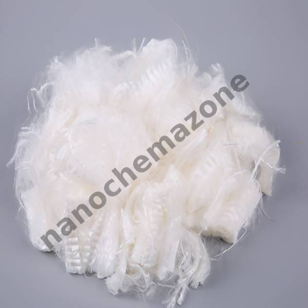
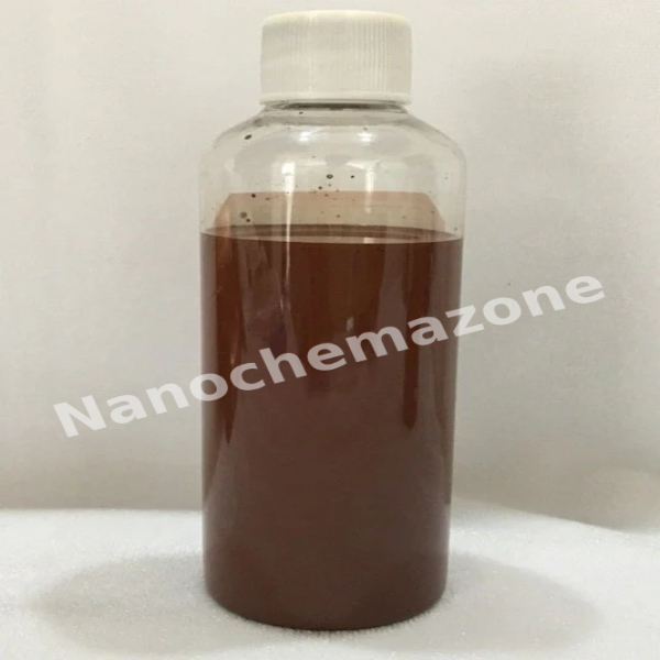
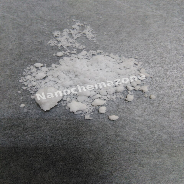
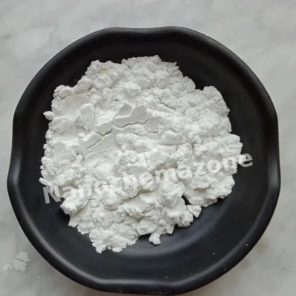
Chitosan(Medical grade) (431668)

$254.00
Select options This product has multiple variants. The options may be chosen on the product page

Product 

Chitosan(Medical grade) (431668)

CAS No.

9012‑76‑4

Appearance

Powder

Purity

≥99%,  ≥99.9%,  ≥95%

(Other purities are also available)

APS

  N/A (Size Can be customized), Ask for other available size ranges.

Ingredient

N/A

Molecular Weight

 161.16 g/mol

Melting Point

 ~102.5 °C

Boiling Point

N/A

Density

 ~1.0 g/cm³

Product Codes

NCZ-2620K

Test Items Specifications
DAC degree ≥ 90%
Protein ≤ 0.2%
Endotoxin ≤ 0.5EU/mg
Heavy metals ≤ 10ppm

Aluminum Oxide (Al2O3) Sputtering Targets, Purity: 99.99%, Size: 1”, Thickness: 0.250”

$255.00

Applications of Sputtering Targets;

Film deposition is accomplished using sputtering targets. A technique for sputtering thin films is called "deposition made by sputter targets," which entails eroding material from a "target" source onto a "substrate" like a silicon wafer. Etching of the target is done using semiconductor sputtering targets. When selectivity is not an issue and a high degree of etching anisotropy is required, sputter etching is the method of choice. By removing the target material through etching, sputter targets are also utilized for investigation. In secondary ion spectroscopy (SIMS), one example is when the target material is sputtered at a steady pace. Mass spectrometry is used to quantify the concentration and identity of spewed atoms as the target is sputtered. With the sputtering target's assistance, the

It is possible to identify the target material and even detect incredibly tiny impurity amounts.

There is also an application area for sputtering targets in space. One type of space weathering that alters the chemical and physical characteristics of airless worlds like the Moon and asteroids is sputtering.

With the chemical formula Al2O3, aluminum oxide is a compound made of aluminum and oxygen. Because of its high melting point, Al2O3 is useful as a refractory material and as an abrasive due to its hardness, as well as for the production of aluminum metal.

Bismuth (Bi) Sputtering Targets, Purity: 99.999%, Size: 2”, Thickness: 0.125”

$255.00

Applications of Sputtering Targets;

Film deposition is accomplished using sputtering targets. A technique for sputtering thin films is called "deposition made by sputter targets," which entails eroding material from a "target" source onto a "substrate" like a silicon wafer. Etching of the target is done using semiconductor sputtering targets. When selectivity is not an issue and a high degree of etching anisotropy is required, sputter etching is the method of choice. By removing the target material through etching, sputter targets are also utilized for investigation. In secondary ion spectroscopy (SIMS), one example is when the target material is sputtered at a steady pace. When the target shatters,

Mass spectrometry measures the concentration and identity of sputtered atoms. The target material's composition may be ascertained and even very low concentrations of contaminants can be found with the aid of the sputtering target.

There is also an application area for sputtering targets in space. One type of space weathering that alters the chemical and physical characteristics of airless worlds like the Moon and asteroids is sputtering.

The metal bismuth is silvery with a hint of pink and is fragile. Both in air and water, it is stable. The thermal and electrical characteristics of bismuth are not good, yet

finds usage in the production of fusible alloys, a class of low-melting-point materials appropriate for a variety of functions, such as thermal fuses and solders. Because pure bismuth exhibits a high absorption of gamma rays, it can be used as a window or filter for these particles while allowing neutrons to pass through.

Due to high thermal conductivity, bimetal can be utilized in a wide range of applications, including heavy metal detection reference electrodes, devices that take use of substantial magneto-resistance, and thermoelectric conversion. Bi also has the intriguing characteristic of turning semi-metal films into semiconductors at a critical thickness of about 30 nm. These films can be deposited using a variety of methods, including laser heat evaporation, RF and DC sputtering, and pulsed deposition. Furthermore, it is significant to note that various authors have reported that the crystalline structure and morphology of Bi coatings deposited through physical vapor deposition (PVD) techniques depend on the deposition parameters, including the substrate's temperature, the potential applied to the target, the energy of the ion beam, and the rate at which energy is released during the ion beam bombardment that deposits the films. Positive pulses applied between the substrate and the target during DC sputtering can modify these parameters, improving the mechanical and density characteristics of the film.

Nickel Chromium (Ni-Cr) Sputtering Targets, Purity: 99.95%, Size: 3”, Thickness: 0.125”

$255.00

Applications of Sputtering Targets;

Film deposition is accomplished using sputtering targets. A technique for sputtering thin films is called "deposition made by sputter targets," which entails eroding material from a "target" source onto a "substrate" like a silicon wafer. Etching of the target is done using semiconductor sputtering targets. When selectivity is not an issue and a high degree of etching anisotropy is required, sputter etching is the method of choice. By removing the target material through etching, sputter targets are also utilized for investigation. In secondary ion spectroscopy (SIMS), one example is when the target material is sputtered at a steady pace. Mass spectrometry is used to quantify the concentration and identity of spewed atoms as the target is sputtered.

The target material's composition may be ascertained and even very low concentrations of contaminants can be found with the aid of the sputtering target.

There is also an application area for sputtering targets in space. One type of space weathering that alters the chemical and physical characteristics of airless worlds like the Moon and asteroids is sputtering.

Nickel Iron (Ni-Fe) Sputtering Targets, Purity: 99.5%, Size: 3”, Thickness: 0.125”

$255.00

Applications of Sputtering Targets;

Film deposition is accomplished using sputtering targets. A technique for sputtering thin films is called "deposition made by sputter targets," which entails eroding material from a "target" source onto a "substrate" like a silicon wafer. Etching of the target is done using semiconductor sputtering targets. When selectivity is not an issue and a high degree of etching anisotropy is required, sputter etching is the method of choice. By removing the target material through etching, sputter targets are also utilized for investigation. In secondary ion spectroscopy (SIMS), one example is when the target material is sputtered at a steady pace. Mass spectrometry is used to quantify the concentration and identity of spewed atoms as the target is sputtered.

The target material's composition may be ascertained and even very low concentrations of contaminants can be found with the aid of the sputtering target.

There is also an application area for sputtering targets in space. One type of space weathering that alters the chemical and physical characteristics of airless worlds like the Moon and asteroids is sputtering.

Silicon Dioxide (SiO2) Sputtering Targets, Fused Quartz, Purity: 99.995%, Size: 8”, Thickness: 0.250”

$255.00

Applications of Sputtering Targets;

Film deposition is accomplished using sputtering targets. A technique for sputtering thin films is called "deposition made by sputter targets," which entails eroding material from a "target" source onto a "substrate" like a silicon wafer. Etching of the target is done using semiconductor sputtering targets. When selectivity is not an issue and a high degree of etching anisotropy is required, sputter etching is the method of choice. By removing the target material through etching, sputter targets are also utilized for investigation. In secondary ion spectroscopy (SIMS), one example is when the target material is sputtered at a steady pace. Mass spectrometry is used to quantify the concentration and identity of spewed atoms as the target is sputtered.

The target material's composition may be ascertained and even very low concentrations of contaminants can be found with the aid of the sputtering target.

There is also an application area for sputtering targets in space. One type of space weathering that alters the chemical and physical characteristics of airless worlds like the Moon and asteroids is sputtering.

Silicon (Si) Sputtering Targets, P-type, Purity: 99.999%, Size: 2”, Thickness: 0.250”

$255.00

Applications of Sputtering Targets;

Film deposition is accomplished using sputtering targets. A technique for sputtering thin films is called "deposition made by sputter targets," which entails eroding material from a "target" source onto a "substrate" like a silicon wafer. Etching of the target is done using semiconductor sputtering targets. When selectivity is not an issue and a high degree of etching anisotropy is required, sputter etching is the method of choice. By removing the target material through etching, sputter targets are also utilized for investigation. In secondary ion spectroscopy (SIMS), one example is when the target material is sputtered at a steady pace. Mass spectrometry is used to quantify the concentration and identity of spewed atoms as the target is sputtered.

The target material's composition may be ascertained and even very low concentrations of contaminants can be found with the aid of the sputtering target.

There is also an application area for sputtering targets in space. One type of space weathering that alters the chemical and physical characteristics of airless worlds like the Moon and asteroids is sputtering.

Tantalum (Ta) Sputtering Targets, Purity: 99.95%, Size: 2”, Thickness: 0.250”

$255.00

Applications of Sputtering Targets;

Film deposition is accomplished using sputtering targets. A technique for sputtering thin films is called "deposition made by sputter targets," which entails eroding material from a "target" source onto a "substrate" like a silicon wafer. Etching of the target is done using semiconductor sputtering targets. When selectivity is not an issue and a high degree of etching anisotropy is required, sputter etching is the method of choice. By removing the target material through etching, sputter targets are also utilized for investigation. In secondary ion spectroscopy (SIMS), one example is when the target material is sputtered at a steady pace. Mass spectrometry is used to quantify the concentration and identity of spewed atoms as the target is sputtered.

The target material's composition may be ascertained and even very low concentrations of contaminants can be found with the aid of the sputtering target.

There is also an application area for sputtering targets in space. One type of space weathering that alters the chemical and physical characteristics of airless worlds like the Moon and asteroids is sputtering.

250 mL Monolayer Graphene Oxide Water Dispersion 2 mg/ml

$255.00
Product 250 mL Monolayer Graphene Oxide Water Dispersion 2 mg/ml
CAS No. 7782-42-5
Appearance Light to dark brown
Purity ≥99%,  ≥99.9%,  ≥95%(Other purities are also available)
APS 0.5–5µm (Size Can be customized),  Ask for other available size range.
Ingredient C₈H₂O₃
Molecular Weight N/A
Melting Point N/A
Boiling Point N/A
Density N/A
Product Codes NCZ-149I
 

Superparamagnetic Iron Oxide Nanoparticle (SPION) High Concentration Suspension

Price range: $255.00 through $1,122.00
Select options This product has multiple variants. The options may be chosen on the product page
Product Superparamagnetic Iron Oxide Nanoparticle (SPION) High Concentration Suspension
CAS No. 1317-61-9
Appearance Dark brown to black opaque liquid
Purity ≥99%,  ≥99.9%,  ≥95%(Other purities are also available)
APS 5–20nm (Size Can be customized),  Ask for other available size range.
Ingredient Fe₃O₄
Molecular Weight N/A
Melting Point N/A
Boiling Point N/A
Density 5.17 g/cm³
Product Codes NCZ-545I
 

Carbon (C) (Graphite) Sputtering Targets, Purity: 99.999%, Size: 4”, Thickness: 0.250”

$255.00

Product 

Carbon (C) (Graphite) Sputtering Targets, Purity: 99.999%, Size: 4'', Thickness: 0.250''

CAS No.

 7782‑42‑5

Appearance

Powder

Purity

≥99%,  ≥99.9%,  ≥95%

(Other purities are also available)

APS

 N/A (Size Can be customized), Ask for other available size ranges.

Ingredient

N/A

Molecular Weight

12.01 g/mol

Melting Point

~3,652 °C (no liquid phase)

Boiling Point

 ~4,200 °C

Density

 ~2.25 g/cm³

Product Codes

NCZ-2349K

Aluminum (Al) Sputtering Targets, Purity: 99.999%, Size: 8”, Thickness: 0.125”

$256.00

 Applications of Sputtering Targets;

  • Sputtering targets is used for film deposition. The deposition made by sputter targets is a method of depositing thin films by sputtering that involves eroding material from a "target" source onto a "substrate" such as  a silicon wafer.
  • Semiconductor sputtering targets is used to etch the target. Sputter etching is chosen in cases where a high degree of etching anisotropy is needed and selectivity is not a concern.
  • Sputter targets is also used for analysis by etching away the target material.
One of the example occurs in secondary ion spectroscopy (SIMS), where the target sample is sputtered at a constant rate. As the target is sputtered, the concentration and identity of sputtered atoms are measured using mass spectrometry. By helping of the sputtering target, the composition of the target material can be determined and even extremely low concentrations of impurities are detected. Sputtering target has also application area in space. Sputtering is one of the forms of space weathering, a process that changes the physical and chemical properties of airless bodies, such as asteroids and the Moon. Aluminum which has the chemical symbol of Al, is a silvery white, soft, ductile metal that is the third most abundant element. Aluminum is notable due to for its light weight, strength, durability and for its ability to resist corrosion. Aluminum forms an extremely thin but very strong layer of oxide film. Aluminum has also high thermal and electrical conductivity. Aluminum sputtering targets have a particularly fine-grained microstructure. This property of Aluminum sputtering targets ensures that you benefit from uniform erosion and a low susceptibility to particle formation throughout the sputtering process.
Zinc Sulfide (ZnS) Sputtering Targets, Purity: 99.99%, Size: 1”, Thickness: 0.125”

$256.00

Product 

Zinc Sulfide (ZnS) Sputtering Targets, Purity: 99.99%, Size: 1'', Thickness: 0.125''

CAS No.

1314-98-3

Appearance

Powder

Purity

≥99%,  ≥99.9%,  ≥95%

(Other purities are also available)

APS

 (ZnS) (Size Can be customized), Ask for other available size ranges.

Ingredient

N/A

Molecular Weight

97.45 g/mol

Melting Point

~1700 °C

Boiling Point

N/A

Density

 4.09 g/cm³

Product Codes

NCZ-1509K

Tin (Sn) Sputtering Targets, Purity: 99.99%, Size: 3”, Thickness: 0.125”

$257.00

Product 

Tin (Sn) Sputtering Targets, Purity: 99.99%, Size: 3'', Thickness: 0.125''

CAS No.

7440-31-5

Appearance

Powder

Purity

≥99%,  ≥99.9%,  ≥95%

(Other purities are also available)

APS

N/A  (Size Can be customized), Ask for other available size ranges.

Ingredient

N/A

Molecular Weight

118.71 g/mol

Melting Point

231.93 °C

Boiling Point

2602 °C

Density

~7.31 g/cm³

Product Codes

NCZ-1641K

Silicon Nitride (Si3N4) Sputtering Targets, Purity: 99.5%, Size: 1”, Thickness: 0.125”, Dark Gray to Black

$258.00

Product 

Silicon Nitride (Si3N4) Sputtering Targets, Purity: 99.5%, Size: 1'', Thickness: 0.125'', Dark Gray to Black

CAS No.

 12033-89-5

Appearance

Powder

Purity

≥99%,  ≥99.9%,  ≥95%

(Other purities are also available)

APS

N/A  (Size Can be customized), Ask for other available size ranges.

Ingredient

N/A

Molecular Weight

 140.28 g/mol

Melting Point

 ~1900 °C

Boiling Point

N/A

Density

~3.2 g/cm³

Product Codes

NCZ-1705K

Niobium Oxide (Nb2O5) Sputtering Targets, Purity: 99.5%, Size: 2”, Thickness: 0.250”

$258.00

Product 

Niobium Oxide (Nb2O5) Sputtering Targets, Purity: 99.5%, Size: 2'', Thickness: 0.250''

CAS No.

1313-96-8

Appearance

Powder

Purity

≥99%,  ≥99.9%,  ≥95%

(Other purities are also available)

APS

N/A (Size Can be customized), Ask for other available size ranges.

Ingredient

N/A

Molecular Weight

 265.81 g/mol

Melting Point

~1512 °C

Boiling Point

N/A

Density

 4.6 – 4.9 g/cm³

Product Codes

NCZ-1809K

Bismuth (Bi) Sputtering Targets, Purity: 99.999%, Size: 1”, Thickness: 0.125”

$258.00

Product 

Bismuth (Bi) Sputtering Targets, Purity: 99.999%, Size: 1'', Thickness: 0.125''

CAS No.

7440‑69‑9

Appearance

Powder

Purity

≥99%,  ≥99.9%,  ≥95%

(Other purities are also available)

APS

1 – 5 µm (Size Can be customized), Ask for other available size ranges.

Ingredient

N/A

Molecular Weight

~208.98 g/mol

Melting Point

 271.4 °C

Boiling Point

~1560 °C

Density

 ~9.78–9.80 g/cm³

Product Codes

NCZ-2440K

Magnetic Graphene Aerogel, Content of Fe3O4: 65%, Diameter: 2±0.4 cm

Price range: $258.50 through $1,199.00
Select options This product has multiple variants. The options may be chosen on the product page
1 piece/ 258.50 € 5 pieces/ 1199 €  Contact us for tailored quotes on larger quantities & experience exceptional solutions from our experts.

Germanium (Ge) Micron Powder, Purity: 99.99 %, Size: 325 mesh

Price range: $259.00 through $1,798.00
Select options This product has multiple variants. The options may be chosen on the product page
25 grams/230 € 100 grams/478 € 500 grams/ 965 € 1000 grams/1595 €
Please contact us for quotes on larger quantities !!!

Germanium (Ge) Micron Powder

Purity: 99.99 %, Size: 325 mesh

Magnetic Graphene Aerogel, Content of Fe3O4: 50%, Diameter: 2±0.4 cm

Price range: $259.00 through $1,204.00
Select options This product has multiple variants. The options may be chosen on the product page
1 piece/ 259 € 5 pieces/ 1204 €  Contact us for tailored quotes on larger quantities & experience exceptional solutions from our experts.

Nickel Vanadium (NiV) Sputtering Targets, Purity: 99.95%, Size: 2”, Thickness: 0.125”

$259.00

Product 

Nickel Vanadium (NiV) Sputtering Targets, Purity: 99.95%, Size: 2'', Thickness: 0.125''

CAS No.

11137-91-4

Appearance

Powder

Purity

≥99%,  ≥99.9%,  ≥95%

(Other purities are also available)

APS

N/A (Size Can be customized), Ask for other available size ranges.

Ingredient

N/A

Molecular Weight

~57.9 g/mol

Melting Point

~1,350–1,450 °C

Boiling Point

N/A

Density

 ~8.5 g/cm³

Product Codes

NCZ-1828K

Manganese (Mn) Sputtering Targets, Purity: 99.95%, Size: 1”, Thickness: 0.125”

$259.00

Product 

Manganese (Mn) Sputtering Targets, Purity: 99.95%, Size: 1'', Thickness: 0.125''

CAS No.

 7439-96-5

Appearance

Powder

Purity

≥99%,  ≥99.9%,  ≥95%

(Other purities are also available)

APS

 N/A (Size Can be customized), Ask for other available size ranges.

Ingredient

N/A

Molecular Weight

54.93804 g/mol

Melting Point

 1,246 °C

Boiling Point

 2,061 °C

Density

 7.21 g/cm³

Product Codes

NCZ-1954K

Magnesium (Mg) Sputtering Targets, Purity: 99.98%, Size: 4”, Thickness: 0.125”

$259.00

Product 

Magnesium (Mg) Sputtering Targets, Purity: 99.98%, Size: 4'', Thickness: 0.125''

CAS No.

7439-95-4

Appearance

Powder

Purity

≥99%,  ≥99.9%,  ≥95%

(Other purities are also available)

APS

 N/A (Size Can be customized), Ask for other available size ranges.

Ingredient

N/A

Molecular Weight

 24.305 g/mol

Melting Point

 650 °C

Boiling Point

 1,090 °C

Density

1.738 g/cm³

Product Codes

NCZ-1994K

Monodisperse Mesoporous Silica Nanosphere (MSN) Stellate, 80 nm

Price range: $259.00 through $517.00
Select options This product has multiple variants. The options may be chosen on the product page
Product Monodisperse Mesoporous Silica Nanosphere (MSN) Stellate, 80 nm
CAS No. 7631-86-9
Appearance White or off-white
Purity ≥99%,  ≥99.9%,  ≥95%(Other purities are also available)
APS 80nm (Size Can be customized),  Ask for other available size range.
Ingredient SiO₂·xH₂O
Molecular Weight N/A
Melting Point N/A
Boiling Point N/A
Density 0.2 – 0.4 g/cm³
Product Codes NCZ-456I
 

Tungsten (W) Nanopowder/Nanoparticles, Purity: 99.955+%, Size: 35-55 nm, Metal Basis

$259.92
Select options This product has multiple variants. The options may be chosen on the product page
Tungsten (W) Nanopowder/Nanoparticles Purity: 99.955+%, Size: 35-55 nm, Metal Basis Technical Properties: True Density (g/cm3) 19,3 Bulk Density (g/cm3) 3,8

Copper Tin (Cu-Sn) Alloy Nanopowder/Nanoparticles, Size: 35-95 nm, Sn:Cu/92:8

Price range: $260.00 through $479.00
Select options This product has multiple variants. The options may be chosen on the product page

Copper Tin (Cu-Sn) Alloy Nanopowder/Nanoparticles

Size:  35-95 nm, Sn:Cu/92:8

Technical Properties:

Alloy Ratio (Sn-Cu) 92-8
Average Particle Size (nm) 35-95

Properties, Storage and Cautions:

Sn-Cu alloy nanoparticles are highly reactive, therefore it should be handled with care and rapid moves, vibrations should be avoided. The powder should be kept away from sunlight, any kind of heating, moisture and impacts. Coagulation of the particles is a serious problem, so, the powder should be sealed under vacuum and should be kept in cool and dry conditions. Air contact should be avoided.

Applications:

Sn-Cu alloy (bronze) is a very old and well known material. It is generally used in bearings, electrical contacts, ship propellers, sculptures, musical instruments and so on…

Copper Tin (Cu-Sn) Alloy Nanopowder/Nanoparticles, Size: 35-95 nm, Sn:Cu/1:9

Price range: $260.00 through $479.00
Select options This product has multiple variants. The options may be chosen on the product page

Copper Tin (Cu-Sn) Alloy Nanopowder/Nanoparticles

Size: 35-95 nm, Sn:Cu/1:9

Technical Properties:

Alloy Ratio (Sn-Cu) 10,0-90,0
Average Particle Size (nm) 35-95

Properties, Storage and Cautions:

Sn-Cu alloy nanoparticles are highly reactive, therefore it should be handled with care and rapid moves, vibrations should be avoided. The powder should be kept away from sunlight, any kind of heating, moisture and impacts. Coagulation of the particles is a serious problem, so, the powder should be sealed under vacuum and should be kept in cool and dry conditions. Air contact should be avoided.

Applications:

Sn-Cu alloy (bronze) is a very old and well known material. It is generally used in bearings, electrical contacts, ship propellers, sculptures, musical instruments and so on…

Multi Walled Carbon Nanotubes N-butanol Dispersion, 4 wt%, Purity: > 96%, OD: 18-28 nm, Length: 8-18 µm

Price range: $260.00 through $1,130.00
Select options This product has multiple variants. The options may be chosen on the product page

Applications:

MWCNTs have numerous potential uses in various industries. Midicine, mechanical, electric, chemical, energy, and other uses are among these. It can be used in a variety of applications, including medication delivery, biosensors, CNT composites, catalysis, nanoprobes, and hydrogen storage. seven lithium battalions tubes for 8 gas discharges, nine-panel flat display, 10-supercapacitor, 11-transistors, twelve solar cells Photoluminescence 13 and template 14

Ultralight Graphene Aerogel, Diameter: 2±0.4 cm, Height: 2±0.4 cm

Price range: $260.00 through $1,039.00
Select options This product has multiple variants. The options may be chosen on the product page
1 piece/ 260 € 5 pieces/ 1039 €  Contact us for tailored quotes on larger quantities & experience exceptional solutions from our experts.

Bismuth (Bi) Sputtering Targets, Purity: 99.999%, Size: 2”, Thickness: 0.250”

$260.00

Applications of Sputtering Targets;

Film deposition is accomplished using sputtering targets. A technique for sputtering thin films is called "deposition made by sputter targets," which entails eroding material from a "target" source onto a "substrate" like a silicon wafer. Etching of the target is done using semiconductor sputtering targets. When selectivity is not an issue and a high degree of etching anisotropy is required, sputter etching is the method of choice. By removing the target material through etching, sputter targets are also utilized for investigation. In secondary ion spectroscopy (SIMS), one example is when the target material is sputtered at a steady pace. Mass spectrometry is used to quantify the concentration and identity of spewed atoms as the target is sputtered. With the sputtering target's assistance, the

It is possible to identify the target material and even detect incredibly tiny impurity amounts.

There is also an application area for sputtering targets in space. One type of space weathering that alters the chemical and physical characteristics of airless worlds like the Moon and asteroids is sputtering.

The metal bismuth is silvery with a hint of pink and is fragile. Both in air and water, it is stable. Despite having poor thermal and electrical qualities, bismuth is used to create fusible alloys, a class of materials with low melting points that can be used in a variety of applications, such as thermal fuses and solders. Because pure bismuth exhibits a strong absorption of gamma rays, it can be used as a window or filter for these at the same time allowing neutrons to flow through.

Germanium Nanoparticles/Nanopowder ( Ge, 200nm)

Price range: $260.00 through $906.00
Select options This product has multiple variants. The options may be chosen on the product page
$260/25g $906/100g

Product 

Germanium Nanoparticles/Nanopowder ( Ge, 200nm)

CAS No.

7440-56-4

Appearance

Powder

Purity

≥99%,  ≥99.9%,  ≥95%

(Other purities are also available)

APS

~200 nm (microns) (Size Can be customized), Ask for other available size ranges.

Ingredient

N/A

Molecular Weight

72.63 g/mol

Melting Point

937.4 °C

Boiling Point

2833 °C

Density

~5.32 g/cm³

Product Codes

NCZ-1047K

3N5 (99.95%) Tungsten (W) Pellets Evaporation Materials

Price range: $260.00 through $1,185.00
Select options This product has multiple variants. The options may be chosen on the product page
Product  3N5 (99.95%) Tungsten (W) Pellets Evaporation Materials
CAS No. 7440-33-7
Appearance Grayish White, Lustrous, Metallic 
Purity ≥99%,  ≥99.9%,  ≥95%(Other purities are also available)
APS 3–6mm (Size Can be customized),  Ask for other available size range.
Ingredient W
Molecular Weight 175.34 g/mol
Melting Point 3,410°C
Boiling Point N/A
Density 19.25 g/cm³
Product Codes NCZ-107E

99.994% (4N4) Potassium Carbonate (K2CO3) Powder

Price range: $260.00 through $1,366.00
Select options This product has multiple variants. The options may be chosen on the product page
Product 99.994% (4N4) Potassium Carbonate (K2CO3) Powder
CAS No. 584-08-7
Appearance White crystalline
Purity ≥99%,  ≥99.9%,  ≥95%(Other purities are also available)
APS 10µm (Size Can be customized),  Ask for other available size range.
Ingredient K2CO3
Molecular Weight 138.205 g/mol
Melting Point N/A
Boiling Point N/A
Density 2.43 g/cm³
Product Codes NCZ-252I
 

Silicon (Si) Sputtering Targets, P-type, indium, Purity: 99.999%, Size: 1”, Thickness: 0.250”

$260.00

Product 

Silicon (Si) Sputtering Targets, P-type, indium, Purity: 99.999%, Size: 1'', Thickness: 0.250''

CAS No.

7440-21-3

Appearance

Powder

Purity

≥99%,  ≥99.9%,  ≥95%

(Other purities are also available)

APS

N/A  (Size Can be customized), Ask for other available size ranges.

Ingredient

N/A

Molecular Weight

28.0855 g/mol

Melting Point

 1,414 °C

Boiling Point

3,265 °C

Density

 2.33 g/cm³

Product Codes

NCZ-1741K

High Purity Tellurium Dioxide (TeO2), 99.9999% 6N

Price range: $260.00 through $1,578.00
Select options This product has multiple variants. The options may be chosen on the product page
Product High Purity Tellurium Dioxide (TeO2), 99.9999% 6N
CAS No. 7446-07-3
Appearance White to pale cream crystalline
Purity ≥99%,  ≥99.9%,  ≥95%(Other purities are also available)
APS N/A
Ingredient TeO2
Molecular Weight 159.60 g/mol
Melting Point N/A
Boiling Point N/A
Density N/A
Product Codes NCZ-413I

Neodymium (III) Oxide (Nd2O3) 99.999% 5N Powder

Price range: $260.00 through $2,136.00
Select options This product has multiple variants. The options may be chosen on the product page
Product Neodymium (III) Oxide (Nd2O3) 99.999% 5N Powder
CAS No. 2037-29-5
Appearance White to off-white
Purity ≥99%,  ≥99.9%,  ≥95%(Other purities are also available)
APS 1–10 nm (Size Can be customized),  Ask for other available size range.
Ingredient Nd2O3
Molecular Weight 336.48 g/mol
Melting Point N/A
Boiling Point N/A
Density 7.24 g/cm³
Product Codes NCZ-470I

Copper Tin (Cu-Sn) Alloy Nanopowder/Nanoparticles, Size: 35-95 nm, Sn:Cu/92:8

Price range: $261.00 through $480.00
Select options This product has multiple variants. The options may be chosen on the product page

Copper Tin (Cu-Sn) Alloy Nanopowder/Nanoparticles

Size:  35-95 nm, Sn:Cu/92:8

Technical Properties:

Alloy Ratio (Sn-Cu) 92-8
Average Particle Size (nm) 35-95

Properties, Storage and Cautions:

Sn-Cu alloy nanoparticles are highly reactive, therefore it should be handled with care and rapid moves, vibrations should be avoided. The powder should be kept away from sunlight, any kind of heating, moisture and impacts. Coagulation of the particles is a serious problem, so, the powder should be sealed under vacuum and should be kept in cool and dry conditions. Air contact should be avoided.

Copper Tin (Cu-Sn) Alloy Nanopowder/Nanoparticles, Size: 35-95 nm, Sn:Cu/92:8

Price range: $261.00 through $480.00
Select options This product has multiple variants. The options may be chosen on the product page
25 grams/230 € 100 grams/338 €
500 grams/423 € 
                      
Please contact us for quotes on larger quantities !!! 

Copper Tin (Cu-Sn) Alloy Nanopowder/Nanoparticles

Size:  35-95 nm, Sn:Cu/92:8

Technical Properties:

Alloy Ratio (Sn-Cu) 92-8
Average Particle Size (nm) 35-95

Properties, Storage and Cautions:

Sn-Cu alloy nanoparticles are highly reactive, therefore it should be handled with care and rapid moves, vibrations should be avoided. The powder should be kept away from sunlight, any kind of heating, moisture and impacts. Coagulation of the particles is a serious problem, so, the powder should be sealed under vacuum and should be kept in cool and dry conditions. Air contact should be avoided.

Applications:

Sn-Cu alloy (bronze) is a very old and well known material. It is generally used in bearings, electrical contacts, ship propellers, sculptures, musical instruments and so on…

Copper Tin (Cu-Sn) Alloy Nanopowder/Nanoparticles, Size: 35-95 nm, Sn:Cu/1:9

Price range: $261.00 through $480.00
Select options This product has multiple variants. The options may be chosen on the product page
25 grams/230 € 100 grams/338 €
500 grams/423 € 
                      
Please contact us for quotes on larger quantities !!! 

Copper Tin (Cu-Sn) Alloy Nanopowder/Nanoparticles

Size: 35-95 nm, Sn:Cu/1:9

Technical Properties:

Alloy Ratio (Sn-Cu) 10,0-90,0
Average Particle Size (nm) 35-95

Properties, Storage and Cautions:

Sn-Cu alloy nanoparticles are highly reactive, therefore it should be handled with care and rapid moves, vibrations should be avoided. The powder should be kept away from sunlight, any kind of heating, moisture and impacts. Coagulation of the particles is a serious problem, so, the powder should be sealed under vacuum and should be kept in cool and dry conditions. Air contact should be avoided.

Applications:

Sn-Cu alloy (bronze) is a very old and well known material. It is generally used in bearings, electrical contacts, ship propellers, sculptures, musical instruments and so on…

Aluminum (Al) Sputtering Targets, Purity: 99.999%, Size: 8”, Thickness: 0.250”

$261.00

Applications of Sputtering Targets;

  • Sputtering targets is used for film deposition. The deposition made by sputter targets is a method of depositing thin films by sputtering that involves eroding material from a "target" source onto a "substrate" such as  a silicon wafer.
  • Semiconductor sputtering targets is used to etch the target. Sputter etching is chosen in cases where a high degree of etching anisotropy is needed and selectivity is not a concern.
  • Sputter targets is also used for analysis by etching away the target material.
One of the example occurs in secondary ion spectroscopy (SIMS), where the target sample is sputtered at a constant rate. As the target is sputtered, the concentration and identity of sputtered atoms are measured using mass spectrometry. By helping of the sputtering target, the composition of the target material can be determined and even extremely low concentrations of impurities are detected. Sputtering target has also application area in space. Sputtering is one of the forms of space weathering, a process that changes the physical and chemical properties of airless bodies, such as asteroids and the Moon. Aluminum which has the chemical symbol of Al, is a silvery white, soft, ductile metal that is the third most abundant element. Aluminum is notable due to for its light weight, strength, durability and for its ability to resist corrosion. Aluminum forms an extremely thin but very strong layer of oxide film. Aluminum has also high thermal and electrical conductivity. Aluminum sputtering targets have a particularly fine-grained microstructure. This property of Aluminum sputtering targets ensures that you benefit from uniform erosion and a low susceptibility to particle formation throughout the sputtering process.
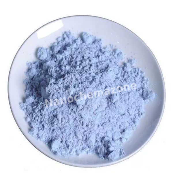
Lithium Titanate (Li2TiO3) Sputtering Targets, Purity: 99.95%, Size: 2”, Thickness: 0.125”

$261.00

Applications of Sputtering Targets;

Film deposition is accomplished using sputtering targets. A technique for sputtering thin films is called "deposition made by sputter targets," which entails eroding material from a "target" source onto a "substrate" like a silicon wafer. Etching of the target is done using semiconductor sputtering targets. When selectivity is not an issue and a high degree of etching anisotropy is required, sputter etching is the method of choice. By removing the target material through etching, sputter targets are also utilized for investigation. In secondary ion spectroscopy (SIMS), one example is when the target material is sputtered at a steady pace. Mass spectrometry is used to quantify the concentration and identity of spewed atoms as the target is sputtered.

By helping of the sputtering target, the composition of the target material may be evaluated and even extremely tiny amounts of contaminants are recognized.

There is also an application area for sputtering targets in space. One type of space weathering that alters the chemical and physical characteristics of airless worlds like the Moon and asteroids is sputtering.

Silicon (Si) Sputtering Targets, P-type, Purity: 99.999%, Size: 3”, Thickness: 0.125”

$261.00

Applications of Sputtering Targets;

Film deposition is accomplished using sputtering targets. A technique for sputtering thin films is called "deposition made by sputter targets," which entails eroding material from a "target" source onto a "substrate" like a silicon wafer. Etching of the target is done using semiconductor sputtering targets. When selectivity is not an issue and a high degree of etching anisotropy is required, sputter etching is the method of choice. By removing the target material through etching, sputter targets are also utilized for investigation. In secondary ion spectroscopy (SIMS), one example is when the target material is sputtered at a steady pace. Mass spectrometry is used to quantify the concentration and identity of spewed atoms as the target is sputtered.

The target material's composition may be ascertained and even very low concentrations of contaminants can be found with the aid of the sputtering target.

There is also an application area for sputtering targets in space. One type of space weathering that alters the chemical and physical characteristics of airless worlds like the Moon and asteroids is sputtering.

Selenium (Se) Sputtering Target

Price range: $261.00 through $923.00
Select options This product has multiple variants. The options may be chosen on the product page

Product 

Selenium (Se) Sputtering Target

CAS No.

7782‑49‑2

Appearance

Powder

Purity

≥99%,  ≥99.9%,  ≥95%

(Other purities are also available)

APS

 NA (Size Can be customized), Ask for other available size ranges.

Ingredient

N/A

Molecular Weight

~78.96 u/g·mol

Melting Point

~217 °C

Boiling Point

~685 °C

Density

~4.79 g/cm³

Product Codes

NCZ-1303K

Tungsten (W) Sputtering Targets, Purity: 99.95%, Size: 3”, Thickness: 0.125”

$261.00

Product 

Tungsten (W) Sputtering Targets, Purity: 99.95%, Size: 3'', Thickness: 0.125''

CAS No.

7440-33-7

Appearance

Powder

Purity

≥99%,  ≥99.9%,  ≥95%

(Other purities are also available)

APS

N/A  (Size Can be customized), Ask for other available size ranges.

Ingredient

N/A

Molecular Weight

 183.84 g/mol

Melting Point

3422 °C

Boiling Point

 5555 °C

Density

19.25 g/cm³

Product Codes

NCZ-1591K

Copper Tin (Cu-Sn) Alloy Nanopowder/Nanoparticles, Size: 35-95 nm, Sn:Cu/92:8

Price range: $261.06 through $480.12
Select options This product has multiple variants. The options may be chosen on the product page
Copper Tin (Cu-Sn) Alloy Nanopowder/Nanoparticles Size:  35-95 nm, Sn:Cu/92:8 Technical Properties: Alloy Ratio (Sn-Cu) 92-8 Average Particle Size (nm) 35-95

Copper Tin (Cu-Sn) Alloy Nanopowder/Nanoparticles, Size: 35-95 nm, Sn:Cu/1:9

Price range: $261.06 through $480.12
Select options This product has multiple variants. The options may be chosen on the product page
Copper Tin (Cu-Sn) Alloy Nanopowder/Nanoparticles Size: 35-95 nm, Sn:Cu/1:9 Technical Properties: Alloy Ratio (Sn-Cu) 10,0-90,0 Average Particle Size (nm) 35-95

Aluminum Foil for Battery Cathode Substrate, Size: 350 m*280 mm*15 µm

Price range: $263.00 through $5,313.00
Select options This product has multiple variants. The options may be chosen on the product page
1 piece/263 € 5 pieces/1182 € 25 pieces/5313 € Please contact us for quotes on larger quantities !!! Aluminum Foil for Battery Cathode Substrate

Aluminum Foil for Battery Cathode Substrate, Size: 350 m*280 mm*15 µm

Price range: $263.00 through $5,313.00
Select options This product has multiple variants. The options may be chosen on the product page
1 piece/263 € 5 pieces/1182 € 25 pieces/5313 € Please contact us for quotes on larger quantities !!! Aluminum Foil for Battery Cathode Substrate

Vanadium (V) Micron Powder Purity: 99.9 %, Size: 100 mesh

Price range: $264.00 through $3,934.00
Select options This product has multiple variants. The options may be chosen on the product page
 25 grams/235 €  100 grams/595 € 500 grams/2140 € 1000 grams/3490 €

Indium (In) Sputtering Targets, Purity: 99.999%, Size: 1”, Thickness: 0.250”

$264.00

Applications of Sputtering Targets;

Film deposition is accomplished using sputtering targets. A technique for sputtering thin films is called "deposition made by sputter targets," which entails eroding material from a "target" source onto a "substrate" like a silicon wafer. Etching of the target is done using semiconductor sputtering targets. When selectivity is not an issue and a high degree of etching anisotropy is required, sputter etching is the method of choice. By removing the target material through etching, sputter targets are also utilized for investigation. In secondary ion spectroscopy (SIMS), one example is when the target material is sputtered at a steady pace. Mass spectrometry is used to quantify the concentration and identity of spewed atoms as the target is sputtered.

The target material's composition may be ascertained and even very low concentrations of contaminants can be found with the aid of the sputtering target.

There is also an application area for sputtering targets in space. One type of space weathering that alters the chemical and physical characteristics of airless worlds like the Moon and asteroids is sputtering.

3N (99.9%) Cerium (Ce) Pieces Evaporation Materials

Price range: $264.00 through $841.00
Select options This product has multiple variants. The options may be chosen on the product page
Product 3N (99.9%) Cerium (Ce) Pieces Evaporation Materials
CAS No. 1313-27-5
Appearance Silvery White, Metallic 
Purity ≥99%,  ≥99.9%,  ≥95%(Other purities are also available)
APS 3mm (Size Can be customized),  Ask for other available size range.
Ingredient Ce
Molecular Weight 143.95 g/mol
Melting Point 798 °C
Boiling Point 3,360 °C
Density 4.69 g/cm³
Product Codes NCZ-133E

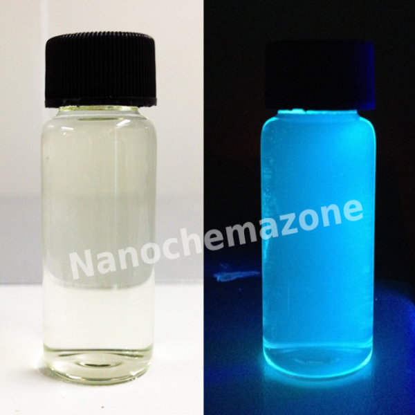
B-doped Graphene Quantum Dots Solution (Blue Fluorescence)

Price range: $264.00 through $459.00
Select options This product has multiple variants. The options may be chosen on the product page
Product B-doped Graphene Quantum Dots Solution (Blue Fluorescence)
CAS No. 1034343-98-0
Appearance Clear to pale yellow or light brown
Purity ≥99%,  ≥99.9%,  ≥95%(Other purities are also available)
APS 4–6nm (Size Can be customized),  Ask for other available size range.
Ingredient B20C980​
Molecular Weight 12.01 g/mol
Melting Point N/A
Boiling Point N/A
Density 1.0–1.1 g/cm³
Product Codes NCZ-293I
 

Gadolinium Chloride Hexahydrate (GdCl3 · 6H2O) 99.9% 3N

$264.00
Select options This product has multiple variants. The options may be chosen on the product page
Product Gadolinium Chloride Hexahydrate (GdCl3 · 6H2O) 99.9% 3N
CAS No. 13450-84-5
Appearance White crystalline
Purity ≥99%,  ≥99.9%,  ≥95%(Other purities are also available)
APS 40–60µm (Size Can be customized),  Ask for other available size range.
Ingredient GdCl3·6H2O
Molecular Weight 371.7 g/mol
Melting Point 609 °C
Boiling Point 1,580 °C
Density 7.07 g/cm³
Product Codes NCZ-350I

High Purity Antimony (III) Oxide (Sb2O3) Powder 99.995% 4N5

$264.00
Select options This product has multiple variants. The options may be chosen on the product page
Product High Purity Antimony (III) Oxide (Sb2O3) Powder 99.995% 4N5
CAS No. 1309-64-4
Appearance White crystalline
Purity ≥99%,  ≥99.9%,  ≥95%(Other purities are also available)
APS N/A
Ingredient Sb2O3
Molecular Weight 291.52 g/mol
Melting Point N/A
Boiling Point N/A
Density 5.2–5.7 g/cm³
Product Codes NCZ-405I

Thulium Chloride Hexahydrate (TmCl3 · 6H2O) 99.95% 3N5

$264.00
Select options This product has multiple variants. The options may be chosen on the product page
Product Thulium Chloride Hexahydrate (TmCl3 · 6H2O) 99.95% 3N5
CAS No. 13461-29-7
Appearance Light pink to pale violet crystalline
Purity ≥99%,  ≥99.9%,  ≥95%(Other purities are also available)
APS 5–50µm (Size Can be customized),  Ask for other available size range.
Ingredient TmCl3·6H2O
Molecular Weight 354.26 g/mol
Melting Point N/A
Boiling Point N/A
Density 1.98 g/cm³
Product Codes NCZ-556I
 

Nickel Vanadium (NiV) Sputtering Targets, Purity: 99.95%, Size: 3”, Thickness: 0.125”

$265.00

Applications of Sputtering Targets;

Film deposition is accomplished using sputtering targets. A technique for sputtering thin films is called "deposition made by sputter targets," which entails eroding material from a "target" source onto a "substrate" like a silicon wafer. Etching of the target is done using semiconductor sputtering targets. When selectivity is not an issue and a high degree of etching anisotropy is required, sputter etching is the method of choice. By removing the target material through etching, sputter targets are also utilized for investigation. In secondary ion spectroscopy (SIMS), one example is when the target material is sputtered at a steady pace. Mass spectrometry is used to quantify the concentration and identity of spewed atoms as the target is sputtered.

The target material's composition may be ascertained and even very low concentrations of contaminants can be found with the aid of the sputtering target.

There is also an application area for sputtering targets in space. One type of space weathering that alters the chemical and physical characteristics of airless worlds like the Moon and asteroids is sputtering.

Silicon Nitride (Si3N4) Sputtering Targets, Purity: 99.5%, Size: 1”, Thickness: 0.250”, Dark Gray to Black

$265.00

Applications of Sputtering Targets;

Film deposition is accomplished using sputtering targets. A technique for sputtering thin films is called "deposition made by sputter targets," which entails eroding material from a "target" source onto a "substrate" like a silicon wafer. Etching of the target is done using semiconductor sputtering targets. When selectivity is not an issue and a high degree of etching anisotropy is required, sputter etching is the method of choice. By removing the target material through etching, sputter targets are also utilized for investigation. In secondary ion spectroscopy (SIMS), one example is when the target material is sputtered at a steady pace. Mass spectrometry is used to quantify the concentration and identity of spewed atoms as the target is sputtered.

The target material's composition may be ascertained and even very low concentrations of contaminants can be found with the aid of the sputtering target.

There is also an application area for sputtering targets in space. One type of space weathering that alters the chemical and physical characteristics of airless worlds like the Moon and asteroids is sputtering.

Silicon (Si) Sputtering Targets, P-type, Purity: 99.999%, Size: 3”, Thickness: 0.250”

$265.00

Applications of Sputtering Targets;

Film deposition is accomplished using sputtering targets. A technique for sputtering thin films is called "deposition made by sputter targets," which entails eroding material from a "target" source onto a "substrate" like a silicon wafer. Etching of the target is done using semiconductor sputtering targets. When selectivity is not an issue and a high degree of etching anisotropy is required, sputter etching is the method of choice. By removing the target material through etching, sputter targets are also utilized for investigation. In secondary ion spectroscopy (SIMS), one example is when the target material is sputtered at a steady pace. Mass spectrometry is used to quantify the concentration and identity of spewed atoms as the target is sputtered.

The target material's composition may be ascertained and even very low concentrations of contaminants can be found with the aid of the sputtering target.

There is also an application area for sputtering targets in space. One type of space weathering that alters the chemical and physical characteristics of airless worlds like the Moon and asteroids is sputtering.

Tungsten Titanium (TiW) Sputtering Targets, Purity: 99.99%, Size: 2”, Thickness: 0.125”

$265.00

Applications of Sputtering Targets;

Film deposition is accomplished using sputtering targets. A technique for sputtering thin films is called "deposition made by sputter targets," which entails eroding material from a "target" source onto a "substrate" like a silicon wafer. Etching of the target is done using semiconductor sputtering targets. When selectivity is not an issue and a high degree of etching anisotropy is required, sputter etching is the method of choice. By removing the target material through etching, sputter targets are also utilized for investigation. In secondary ion spectroscopy (SIMS), one example is when the target material is sputtered at a steady pace. Mass spectrometry is used to quantify the concentration and identity of spewed atoms as the target is sputtered.

The target material's composition may be ascertained and even very low concentrations of contaminants can be found with the aid of the sputtering target.

There is also an application area for sputtering targets in space. One type of space weathering that alters the chemical and physical characteristics of airless worlds like the Moon and asteroids is sputtering.

250 ml Monolayer Graphene Oxide Water Dispersion 4 mg/ml

$265.00
Product 250 ml Monolayer Graphene Oxide Water Dispersion 4 mg/ml
CAS No. 7782-42-5
Appearance White Liquid
Purity ≥99%,  ≥99.9%,  ≥95%(Other purities are also available)
APS 0.5–5µm (Size Can be customized),  Ask for other available size range.
Ingredient CₓHᵧO
Molecular Weight N/A
Melting Point N/A
Boiling Point N/A
Density N/A
Product Codes NCZ-148I