Lanthanum Hexaboride Nanoparticles/ Nanopowder (LaB6, 99+%, 50-80 nm)

Price range: $233.00 through $681.00
Select options This product has multiple variants. The options may be chosen on the product page
$233/25g $394/50g $681/100g
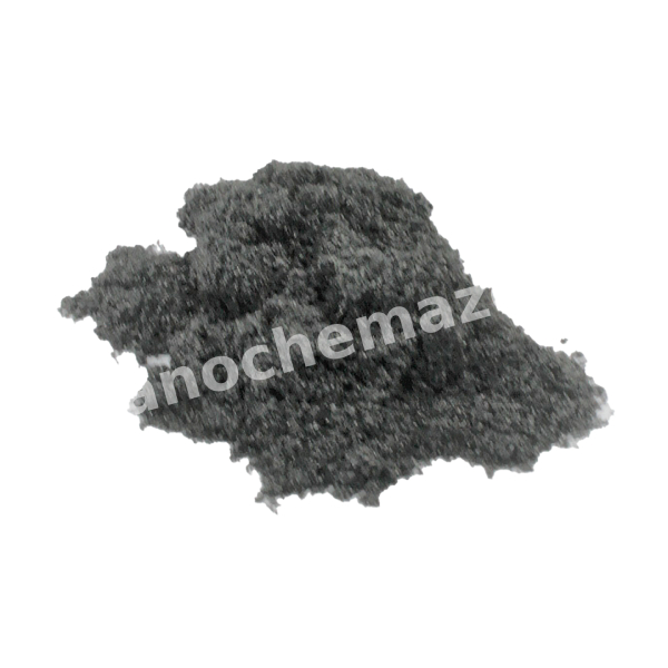
Product Lanthanum Hexaboride Nanoparticles/ Nanopowder (LaB6, 99+%, 50-80 nm)
CAS No. 12008-21-8
Appearance Black powder
Purity ≥99%,  ≥99.9%,  ≥95%(Other purities are also available)
APS 50-80nm (Size Can be customized),  Ask for other available size range.
Ingredient LaB6
Molecular Weight 203.78g/mol
Melting Point 2210°C
Boiling Point N/A
Density 4.72 g/cm³
Product Codes NCZ-115R
 

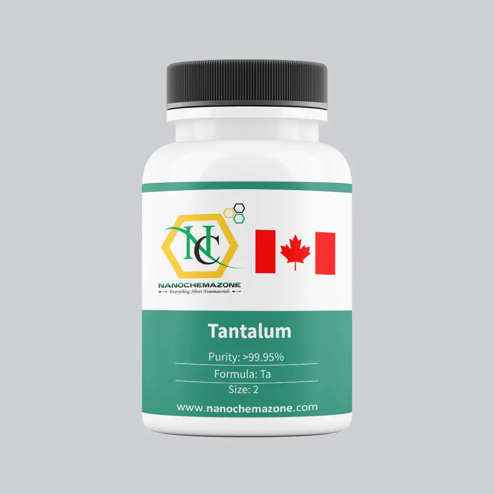
Tantalum (Ta) Sputtering Targets, Purity: 99.95%, Size: 1”, Thickness: 0.250”

$233.00

Product 

Tantalum (Ta) Sputtering Targets, Purity: 99.95%, Size: 1'', Thickness: 0.250''

CAS No.

 7440-25-7

Appearance

Powder

Purity

≥99%,  ≥99.9%,  ≥95%

(Other purities are also available)

APS

N/A  (Size Can be customized), Ask for other available size ranges.

Ingredient

N/A

Molecular Weight

 180.95 g/mol

Melting Point

3017 °C

Boiling Point

 5458 °C

Density

16.65 g/cm³

Product Codes

NCZ-1666K

Magnesium (Mg) Sputtering Targets, Purity: 99.98%, Size: 2”, Thickness: 0.250”

$233.00

Product 

Magnesium (Mg) Sputtering Targets, Purity: 99.98%, Size: 2'', Thickness: 0.250''

CAS No.

7439-95-4

Appearance

Powder

Purity

≥99%,  ≥99.9%,  ≥95%

(Other purities are also available)

APS

 N/A (Size Can be customized), Ask for other available size ranges.

Ingredient

N/A

Molecular Weight

 24.305 g/mol

Melting Point

 650 °C

Boiling Point

 1,090 °C

Density

1.738 g/cm³

Product Codes

NCZ-2000K

Silicon Dioxide (SiO2) Sputtering Targets, Fused Quartz, Purity: 99.995%, Size: 6”, Thickness: 0.125”

$235.00

Applications of Sputtering Targets;

Film deposition is accomplished using sputtering targets. A technique for sputtering thin films is called "deposition made by sputter targets," which entails eroding material from a "target" source onto a "substrate" like a silicon wafer. Etching of the target is done using semiconductor sputtering targets. When selectivity is not an issue and a high degree of etching anisotropy is required, sputter etching is the method of choice. By removing the target material through etching, sputter targets are also utilized for investigation. In secondary ion spectroscopy (SIMS), one example is when the target material is sputtered at a steady pace. Mass spectrometry is used to quantify the concentration and identity of spewed atoms as the target is sputtered.

The target material's composition may be ascertained and even very low concentrations of contaminants can be found with the aid of the sputtering target.

There is also an application area for sputtering targets in space. One type of space weathering that alters the chemical and physical characteristics of airless worlds like the Moon and asteroids is sputtering.

High Purity Graphene -COOH Functionalized (98%, 1~3nm)

Price range: $235.00 through $985.00
Select options This product has multiple variants. The options may be chosen on the product page
$235/1g $985/5g
Product High Purity Graphene -COOH Functionalized  (98%, 1~3nm)
CAS No. N/A
Appearance Black powder
Purity ≥99%,  ≥99.9%,  ≥95%(Other purities are also available)
APS 1-3nm (Size Can be customized),  Ask for other available size range.
Ingredient C(1-x)O(x/2)(OH)(y)(-COOH)z
Molecular Weight N/A
Melting Point 3697 °C
Boiling Point 4200 °C
Density N/A
Product Codes NCZ-103G
 

High Purity Graphene -N2 Functionalized (98%, 1~3nm)

Price range: $235.00 through $845.00
Select options This product has multiple variants. The options may be chosen on the product page
$235/1g $845/5g
Product High Purity Graphene -N2 Functionalized (98%, 1~3nm)
CAS No. 1034343-98-0
Appearance Black powder
Purity ≥99%,  ≥99.9%,  ≥95%(Other purities are also available)
APS 1-3nm (Size Can be customized),  Ask for other available size range.
Ingredient N/A
Molecular Weight N/A
Melting Point 3697 °C
Boiling Point 4200 °C
Density N/A
Product Codes NCZ-104G
 

Permalloy (Ni-Fe-Mo) Sputtering Targets, Size: 2”, Thickness: 0.125”

$235.00

Product 

Permalloy (Ni-Fe-Mo) Sputtering Targets, Size: 2'', Thickness: 0.125''

CAS No.

 Nickel: 7440-02-0 Iron: 7439-89-6 Molybdenum: 7439-98-7

Appearance

Powder

Purity

≥99%,  ≥99.9%,  ≥95%

(Other purities are also available)

APS

N/A (Size Can be customized), Ask for other available size ranges.

Ingredient

N/A

Molecular Weight

 Not defined (alloy), but elemental weights: Ni: 58.69 g/mol Fe: 55.85 g/mol Mo: 95.95 g/mol

Melting Point

 ~1450 °C

Boiling Point

 ~2730–3000 °C

Density

~8.7 g/cm³

Product Codes

NCZ-1801K

Thin Graphene Nanoplatelets, 1g

$235.00
Product Thin Graphene Nanoplatelets, 1g
CAS No. 1034343-98-0
Appearance Black to dark gray
Purity ≥99%,  ≥99.9%,  ≥95%(Other purities are also available)
APS 0.5–25µm  (Size Can be customized),  Ask for other available size range.
Ingredient C
Molecular Weight Black to dark gray
Melting Point N/A
Boiling Point N/A
Density 2.2 g/cm³
Product Codes NCZ-554I

Aluminum (Al) Sputtering Targets, Purity: 99.999%, Size: 6”, Thickness: 0.250”

$236.00

Applications of Sputtering Targets;

  • Sputtering targets is used for film deposition. The deposition made by sputter targets is a method of depositing thin films by sputtering that involves eroding material from a "target" source onto a "substrate" such as  a silicon wafer.
  • Semiconductor sputtering targets is used to etch the target. Sputter etching is chosen in cases where a high degree of etching anisotropy is needed and selectivity is not a concern.
  • Sputter targets is also used for analysis by etching away the target material.
One of the example occurs in secondary ion spectroscopy (SIMS), where the target sample is sputtered at a constant rate. As the target is sputtered, the concentration and identity of sputtered atoms are measured using mass spectrometry. By helping of the sputtering target, the composition of the target material can be determined and even extremely low concentrations of impurities are detected. Sputtering target has also application area in space. Sputtering is one of the forms of space weathering, a process that changes the physical and chemical properties of airless bodies, such as asteroids and the Moon. Aluminum which has the chemical symbol of Al, is a silvery white, soft, ductile metal that is the third most abundant element. Aluminum is notable due to for its light weight, strength, durability and for its ability to resist corrosion. Aluminum forms an extremely thin but very strong layer of oxide film. Aluminum has also high thermal and electrical conductivity. Aluminum sputtering targets have a particularly fine-grained microstructure. This property of Aluminum sputtering targets ensures that you benefit from uniform erosion and a low susceptibility to particle formation throughout the sputtering process.

Gallium Arsenide (GaAs) Wafer, Size: 4”, Thickness: 300± 25 μm, Double Side Polished, EPI-ready

Price range: $237.00 through $4,776.00
Select options This product has multiple variants. The options may be chosen on the product page
Gallium Arsenide (GaAs) Wafer Size: 4”, Double Side Polished, Thickness: 300± 25 μm, EPI-ready Technical Properties: Quality  GaAs Materials  GaAs

Permalloy (Ni-Fe-Mo) Sputtering Targets, Size: 2”, Thickness: 0.250”

$237.00

Applications of Sputtering Targets;

Film deposition is done using sputtering targets. One technique for sputtering thin films is called "sputter target deposition," which entails eroding material from a "target" source onto a "substrate," such a silicon wafer. The target is etched using semiconductor sputtering targets. When selectivity is unimportant and a high degree of etching anisotropy is required, sputter etching is the method of choice. By removing the target material by etching, sputter targets are also employed in analysis. One instance is in secondary ion spectroscopy (SIMS), in which the target sample is bombarded continuously. Mass spectrometry is used to quantify the concentration and identity of sputtered atoms while the target is sputtered.

The target material's composition may be ascertained and even very low concentrations of contaminants can be found with the aid of the sputtering target.

There is also an application area for sputtering targets in space. One type of space weathering that alters the chemical and physical characteristics of airless worlds like the Moon and asteroids is sputtering.

Silicon Nitride (Si3N4) Sputtering Targets, Purity: 99.9%, Size: 1”, Thickness: 0.125”, White to Gray

$237.00

Applications of Sputtering Targets;

Film deposition is accomplished using sputtering targets. A technique for sputtering thin films is called "deposition made by sputter targets," which entails eroding material from a "target" source onto a "substrate" like a silicon wafer. Etching of the target is done using semiconductor sputtering targets. When selectivity is not an issue and a high degree of etching anisotropy is required, sputter etching is the method of choice. By removing the target material through etching, sputter targets are also utilized for investigation. In secondary ion spectroscopy (SIMS), one example is when the target material is sputtered at a steady pace. Mass spectrometry is used to quantify the concentration and identity of spewed atoms as the target is sputtered.

The target material's composition may be ascertained and even very low concentrations of contaminants can be found with the aid of the sputtering target.

There is also an application area for sputtering targets in space. One type of space weathering that alters the chemical and physical characteristics of airless worlds like the Moon and asteroids is sputtering.

Silicon Sputtering Target Si N-Type

Price range: $237.00 through $523.00
Select options This product has multiple variants. The options may be chosen on the product page
Product Silicon Sputtering Target Si N-Type
CAS No. 7440-21-3
Appearance Dark Gray with a Bluish Tinge, Semi-Metallic
Purity ≥99%,  ≥99.9%,  ≥95% (Other purities are also available)
APS 1–20µm (Size Can be customized),  Ask for other available size range.
Ingredient Si
Molecular Weight 28.0855 g/mol
Melting Point 1,410 °C
Boiling Point 2,355 °C
Density 2.33 g/cm³
Product Codes NCZ-137H
 

Silicon Sputtering Target Si P-Type

Price range: $237.00 through $494.00
Select options This product has multiple variants. The options may be chosen on the product page
Product Silicon Sputtering Target Si P-Type
CAS No. 7440-21-3
Appearance Dark Gray with a Bluish Tinge, Semi-Metallic
Purity ≥99%,  ≥99.9%,  ≥95%(Other purities are also available)
APS 1–20µm (Size Can be customized),  Ask for other available size range.
Ingredient Si
Molecular Weight 28.0855 g/mol
Melting Point N/A
Boiling Point N/A
Density 2.33 g/cm³
Product Codes NCZ-138H

CR2016 Coin Cell Cases with 316SS (Positive+Negative Cases), Diameter: 20 mm, Height : 1.6 mm

Price range: $238.00 through $1,863.00
Select options This product has multiple variants. The options may be chosen on the product page
100 set:238€ 500 set: 1038€ 1000 set:1863€ Technical Properties: Diameter 20 mm Height 1.6 mm Material 316SS

CR2450 Coin Cell Cases with 316SS (Positive+Negative Cases), Diameter: 24 mm, Height : 5 mm

Price range: $238.00 through $1,863.00
Select options This product has multiple variants. The options may be chosen on the product page
100 set:238€ 500 set: 1038€ 1000 set:1863€ Technical Properties: Diameter 24 mm Height 5 mm Material 316SS

Aluminum Silicon (AlSi) Sputtering Targets, Purity: 99.999%, Size: 4”, Thickness: 0.125”

$238.00

Applications of Sputtering Targets;

Film deposition is accomplished using sputtering targets. A technique for sputtering thin films is called "deposition made by sputter targets," which entails eroding material from a "target" source onto a "substrate" like a silicon wafer. Etching of the target is done using semiconductor sputtering targets. When selectivity is not an issue and a high degree of etching anisotropy is required, sputter etching is the method of choice. By removing the target material through etching, sputter targets are also utilized for investigation. In secondary ion spectroscopy (SIMS), one example is when the target material is sputtered at a steady pace. When the target shatters,

Mass spectrometry measures the concentration and identity of sputtered atoms. The target material's composition may be ascertained and even very low concentrations of contaminants can be found with the aid of the sputtering target.

There is also an application area for sputtering targets in space. One type of space weathering that alters the chemical and physical characteristics of airless worlds like the Moon and asteroids is sputtering.

1 kg, 1-2 um Alpha Aluminum Oxide (Alumina) Al2O3 Powder 99.999% 5N

$238.00
Product 1 kg, 1-2 um Alpha Aluminum Oxide (Alumina) Al2O3 Powder 99.999% 5N
CAS No. 1344-28-1
Appearance White
Purity ≥99%,  ≥99.9%,  ≥95%(Other purities are also available)
APS 1-2um (Size Can be customized), Ask for other available size range.
Ingredient Al2O3
Molecular Weight N/A
Melting Point N/A
Boiling Point N/A
Density 3.987 g/cm3
Product Codes NCZ-109I
 

Dysprosium (III) Oxide (Dy2O3) Powder 99.99% 4N

Price range: $238.00 through $2,246.00
Select options This product has multiple variants. The options may be chosen on the product page
Product Dysprosium (III) Oxide (Dy2O3) Powder 99.99% 4N
CAS No. 1308-87-8
Appearance Fine white to pastel yellow–green crystalline
Purity ≥99%,  ≥99.9%,  ≥95%(Other purities are also available)
APS 1–5µm (Size Can be customized),  Ask for other available size range.
Ingredient Dy2O3
Molecular Weight 372.998 g/mol
Melting Point 2 408 °C
Boiling Point N/A
Density 7.80–7.81 g/cm³
Product Codes NCZ-338I

Magnesium (Mg) Sputtering Targets, Purity: 99.98%, Size: 3”, Thickness: 0.125”

$238.00

Product 

Magnesium (Mg) Sputtering Targets, Purity: 99.98%, Size: 3'', Thickness: 0.125''

CAS No.

7439-95-4

Appearance

Powder

Purity

≥99%,  ≥99.9%,  ≥95%

(Other purities are also available)

APS

 N/A (Size Can be customized), Ask for other available size ranges.

Ingredient

N/A

Molecular Weight

 24.305 g/mol

Melting Point

 650 °C

Boiling Point

 1,090 °C

Density

1.738 g/cm³

Product Codes

NCZ-1998K

Antimony (Sb) Sputtering Targets, Purity: 99.999%, Size: 1”, Thickness: 0.250”

$238.00

Product 

Antimony (Sb) Sputtering Targets, Purity: 99.999%, Size: 1'', Thickness: 0.250''

CAS No.

 7440-36-0

Appearance

Powder

Purity

≥99%,  ≥99.9%,  ≥95%

(Other purities are also available)

APS

N/A (Size Can be customized), Ask for other available size ranges.

Ingredient

N/A

Molecular Weight

 121.76 g/mol

Melting Point

 630.6 °C

Boiling Point

 1587 °C

Density

 6.69 g/cm³

Product Codes

NCZ-2510K

Aluminum (Al) Sputtering Targets, Purity: 99.999%, Size: 4”, Thickness: 0.250”

$239.00

Applications of Sputtering Targets;

  • Sputtering targets is used for film deposition. The deposition made by sputter targets is a method of depositing thin films by sputtering that involves eroding material from a "target" source onto a "substrate" such as  a silicon wafer.
  • Semiconductor sputtering targets is used to etch the target. Sputter etching is chosen in cases where a high degree of etching anisotropy is needed and selectivity is not a concern.
  • Sputter targets is also used for analysis by etching away the target material.
One of the example occurs in secondary ion spectroscopy (SIMS), where the target sample is sputtered at a constant rate. As the target is sputtered, the concentration and identity of sputtered atoms are measured using mass spectrometry. By helping of the sputtering target, the composition of the target material can be determined and even extremely low concentrations of impurities are detected. Sputtering target has also application area in space. Sputtering is one of the forms of space weathering, a process that changes the physical and chemical properties of airless bodies, such as asteroids and the Moon. Aluminum which has the chemical symbol of Al, is a silvery white, soft, ductile metal that is the third most abundant element. Aluminum is notable due to for its light weight, strength, durability and for its ability to resist corrosion. Aluminum forms an extremely thin but very strong layer of oxide film. Aluminum has also high thermal and electrical conductivity. Aluminum sputtering targets have a particularly fine-grained microstructure. This property of Aluminum sputtering targets ensures that you benefit from uniform erosion and a low susceptibility to particle formation throughout the sputtering process.

Aluminum (Al) Sputtering Targets, Purity: 99.99%, Size: 6”, Thickness: 0.125”

$239.00

Applications of Sputtering Targets;

  • Sputtering targets is used for film deposition. The deposition made by sputter targets is a method of depositing thin films by sputtering that involves eroding material from a "target" source onto a "substrate" such as  a silicon wafer.
  • Semiconductor sputtering targets is used to etch the target. Sputter etching is chosen in cases where a high degree of etching anisotropy is needed and selectivity is not a concern.
  • Sputter targets is also used for analysis by etching away the target material.
One of the example occurs in secondary ion spectroscopy (SIMS), where the target sample is sputtered at a constant rate. As the target is sputtered, the concentration and identity of sputtered atoms are measured using mass spectrometry. By helping of the sputtering target, the composition of the target material can be determined and even extremely low concentrations of impurities are detected. Sputtering target has also application area in space. Sputtering is one of the forms of space weathering, a process that changes the physical and chemical properties of airless bodies, such as asteroids and the Moon. Aluminum which has the chemical symbol of Al, is a silvery white, soft, ductile metal that is the third most abundant element. Aluminum is notable due to for its light weight, strength, durability and for its ability to resist corrosion. Aluminum forms an extremely thin but very strong layer of oxide film. Aluminum has also high thermal and electrical conductivity. Aluminum sputtering targets have a particularly fine-grained microstructure. This property of Aluminum sputtering targets ensures that you benefit from uniform erosion and a low susceptibility to particle formation throughout the sputtering process.

Silicon Dioxide (SiO2) Sputtering Targets, Fused Quartz, Purity: 99.995%, Size: 4”, Thickness: 0.250”

$239.00

Product 

Silicon Dioxide (SiO2) Sputtering Targets, Fused Quartz, Purity: 99.995%, Size: 4'', Thickness: 0.250''

CAS No.

7631-86-9

Appearance

Powder

Purity

≥99%,  ≥99.9%,  ≥95%

(Other purities are also available)

APS

SiO₂ (Size Can be customized), Ask for other available size ranges.

Ingredient

N/A

Molecular Weight

60.08 g/mol

Melting Point

~1713 °C

Boiling Point

~2230 °C

Density

~2.2 g/cm³

Product Codes

NCZ-1392K

Molybdenum Oxide (MoO3) Sputtering Targets, Purity: 99.9%, Size: 1”, Thickness: 0.125”

$239.00

Product 

Molybdenum Oxide (MoO3) Sputtering Targets, Purity: 99.9%, Size: 1'', Thickness: 0.125''

CAS No.

1313-27-5

Appearance

Powder

Purity

≥99%,  ≥99.9%,  ≥95%

(Other purities are also available)

APS

 N/A (Size Can be customized), Ask for other available size ranges.

Ingredient

N/A

Molecular Weight

 143.94 g/mol

Melting Point

 ~795°C

Boiling Point

 ~1155°C

Density

 ~4.7 g/cm³

Product Codes

NCZ-1904K

Samarium (III) Oxide (Sm2O3) 99.99% 4N Powder

Price range: $239.00 through $580.00
Select options This product has multiple variants. The options may be chosen on the product page
Product Samarium (III) Oxide (Sm2O3) 99.99% 4N Powder
CAS No. 12060-10-1
Appearance White to pale yellow
Purity ≥99%,  ≥99.9%,  ≥95%(Other purities are also available)
APS 1–10µm (Size Can be customized),  Ask for other available size range.
Ingredient Sm2O3
Molecular Weight 348.72 g/mol
Melting Point 2345 °C
Boiling Point N/A
Density 7.52 g/cm³
Product Codes NCZ-507I

Erbium Oxide (Er2O3) Sputtering Targets, Purity: 99.99%, Size: 4”, Thickness: 0.125”

$239.00

Product 

Erbium Oxide (Er2O3) Sputtering Targets, Purity: 99.99%, Size: 4'', Thickness: 0.125''

CAS No.

12061-16-4

Appearance

Powder

Purity

≥99%,  ≥99.9%,  ≥95%

(Other purities are also available)

APS

 N/A (Size Can be customized), Ask for other available size ranges.

Ingredient

N/A

Molecular Weight

382.52 g/mol

Melting Point

~2,343 °C

Boiling Point

N/A

Density

~8.64 g/cm³

Product Codes

NCZ-2244K

CR2325 Coin Cell Cases with 316SS (Positive+Negative Cases), Diameter: 23 mm, Height : 2.5 mm

Price range: $240.00 through $1,860.00
Select options This product has multiple variants. The options may be chosen on the product page
100 set: 240€ 500 set: 1040€ 1000 set:1860€ Technical Properties: Diameter 23 mm Height 2.5 mm Material 316SS

Aluminum (Al) Sputtering Targets, Purity: 99.99%, Size: 8”, Thickness: 0.125”

$240.00

Applications of Sputtering Targets;

  • Sputtering targets is used for film deposition. The deposition made by sputter targets is a method of depositing thin films by sputtering that involves eroding material from a "target" source onto a "substrate" such as  a silicon wafer.
  • Semiconductor sputtering targets is used to etch the target. Sputter etching is chosen in cases where a high degree of etching anisotropy is needed and selectivity is not a concern.
  • Sputter targets is also used for analysis by etching away the target material.
One of the example occurs in secondary ion spectroscopy (SIMS), where the target sample is sputtered at a constant rate. As the target is sputtered, the concentration and identity of sputtered atoms are measured using mass spectrometry. By helping of the sputtering target, the composition of the target material can be determined and even extremely low concentrations of impurities are detected. Sputtering target has also application area in space. Sputtering is one of the forms of space weathering, a process that changes the physical and chemical properties of airless bodies, such as asteroids and the Moon. Aluminum which has the chemical symbol of Al, is a silvery white, soft, ductile metal that is the third most abundant element. Aluminum is notable due to for its light weight, strength, durability and for its ability to resist corrosion. Aluminum forms an extremely thin but very strong layer of oxide film. Aluminum has also high thermal and electrical conductivity. Aluminum sputtering targets have a particularly fine-grained microstructure. This property of Aluminum sputtering targets ensures that you benefit from uniform erosion and a low susceptibility to particle formation throughout the sputtering process.

Bismuth (Bi) Sputtering Targets, Purity: 99.999%, Size: 1”, Thickness: 0.250”

$240.00

Applications of Sputtering Targets;

Film deposition is accomplished using sputtering targets. A technique for sputtering thin films is called "deposition made by sputter targets," which entails eroding material from a "target" source onto a "substrate" like a silicon wafer. Etching of the target is done using semiconductor sputtering targets. When selectivity is not an issue and a high degree of etching anisotropy is required, sputter etching is the method of choice. By removing the target material through etching, sputter targets are also utilized for investigation. In secondary ion spectroscopy (SIMS), one example is when the target material is sputtered at a steady pace. Mass spectrometry is used to quantify the concentration and identity of spewed atoms as the target is sputtered. With the sputtering target's assistance, the It is possible to identify the target material and even detect incredibly tiny impurity amounts. There is also an application area for sputtering targets in space. One type of space weathering that alters the chemical and physical characteristics of airless worlds like the Moon and asteroids is sputtering. The metal bismuth is silvery with a hint of pink and is fragile. Both in air and water, it is stable. Despite having poor thermal and electrical qualities, bismuth is used to create fusible alloys, a class of materials with low melting points that can be used in a variety of applications, such as thermal fuses and solders. Because pure bismuth exhibits a strong absorption of gamma rays, it can be used as a window or filter for these at the same time allowing neutrons to flow through.

Tantalum (Ta) Sputtering Targets, Purity: 99.95%, Size: 2”, Thickness: 0.125”

$240.00

Applications of Sputtering Targets;

Film deposition is accomplished using sputtering targets. A technique for sputtering thin films is called "deposition made by sputter targets," which entails eroding material from a "target" source onto a "substrate" like a silicon wafer. Etching of the target is done using semiconductor sputtering targets. When selectivity is not an issue and a high degree of etching anisotropy is required, sputter etching is the method of choice. By removing the target material through etching, sputter targets are also utilized for investigation. In secondary ion spectroscopy (SIMS), one example is when the target material is sputtered at a steady pace. Mass spectrometry is used to quantify the concentration and identity of spewed atoms as the target is sputtered.

The target material's composition may be ascertained and even very low concentrations of contaminants can be found with the aid of the sputtering target.

There is also an application area for sputtering targets in space. One type of space weathering that alters the chemical and physical characteristics of airless worlds like the Moon and asteroids is sputtering.

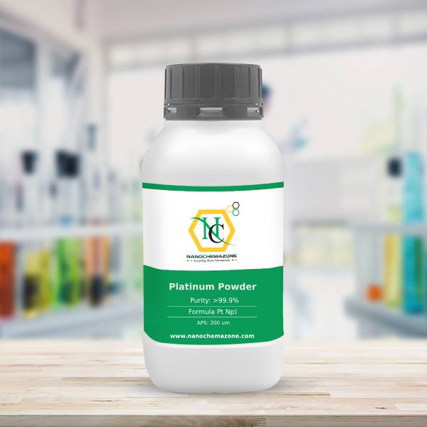
Platinum Nanopowder/Nanoparticles (Pt Np, 99.9%, 200nm)

Price range: $240.00 through $425.00
Select options This product has multiple variants. The options may be chosen on the product page
$240/0.5g
$425/1g

Product 

Platinum Nanopowder/Nanoparticles (Pt Np, 99.9%, 200nm)

CAS No.

7440-06-4

Appearance

Powder

Purity

≥99%,  ≥99.9%,  ≥95%

(Other purities are also available)

APS

200nm (Size Can be customized), Ask for other available size ranges.

Ingredient

N/A

Molecular Weight

195.08 g/mol

Melting Point

1,768 °C

Boiling Point

 3,825 °C

Density

~21.45 g/cm³

Product Codes

NCZ-1061K

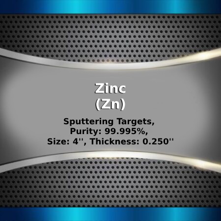
Zinc (Zn) Sputtering Targets, Purity: 99.95%, Size: 4”, Thickness: 0.250”

$240.00

Product 

Zinc (Zn) Sputtering Targets, Purity: 99.95%, Size: 4'', Thickness: 0.250''

CAS No.

7440‑66‑6

Appearance

Powder

Purity

≥99%,  ≥99.9%,  ≥95%

(Other purities are also available)

APS

Zn (black granules) (Size Can be customized), Ask for other available size ranges.

Ingredient

N/A

Molecular Weight

65.38 g/mol

Melting Point

419.5 °C

Boiling Point

 907 °C

Density

7.14 g/cm³

Product Codes

NCZ-1465K

Potassium Iodide (KI) 99.0% High Purity Powder

Price range: $240.00 through $9,365.00
Select options This product has multiple variants. The options may be chosen on the product page
Product Potassium Iodide (KI) 99.0% High Purity Powder
CAS No. 7681-11-0
Appearance White or colorless, odorless
Purity ≥99%,  ≥99.9%,  ≥95%(Other purities are also available)
APS 50–150µm (Size Can be customized),  Ask for other available size range.
Ingredient KI
Molecular Weight 166.00 g/mol
Melting Point 681 °C
Boiling Point N/A
Density 3.13 g/cm³
Product Codes NCZ-497I

Chitosan(from Aspergillus Niger) (237555)

$240.00
Select options This product has multiple variants. The options may be chosen on the product page
Chitosan(from Aspergillus Niger) (237555)
ANALYSIS SPECIFICATION RUSULT
Deacetylation ≥90% 90.18%
Appearance White or yellow powder Complies
Viscosity in 1% Acetic acid ≥15cps 18cps
Mesh size 100% pass 80 mesh Complies
Loss on drying ≤8% 7.2%
Total ash ≤ 2% 0.43%
Heavy Metals ≤20.0ppm 10ppm
As ≤ 2.0ppm 1ppm
Pb ≤ 1.0ppm 0.87ppm
Cd ≤ 0.5ppm Negative
Hg ≤ 0.5ppm Negative
Microbiological quality Total Plate Count Yeast & Mold E.Coli. Salmonella . <1000cfu/g <100cfu/g Negative Negative . 85cfu/g 18cfu/g Negative Negative
  Product Codes- NCZ-2662K

Boron nitride(>99.3%, 6-55μm) (355673)

$240.00
Boron nitride(>99.3%, 6-55μm) (355673)
Grade BN (%) B2O3 (%) C (%) Total oxygen (%) Si, Al, Ca, Cu, K, Fe, Na, Ni, Cr (ppm) D50(μm) BET(m2/g) Tap Density(g/cm3)
TW06 >99.3 <0.3 <0.04 <0.6 <10 each 6-8 4-8 0.40-0.60
TW10 >99.5 <0.2 <0.04 <0.5 <10 each 9-12 4-8 0.35-0.50
TW15 >99.5 <0.2 <0.04 <0.5 <10 each 13-17 3-6 0.35-0.50
TW20 >99.5 <0.2 <0.04 <0.5 <10 each 17-21 3-6 0.35-0.50
TW50 >99.5 <0.2 <0.04 <0.5 <10 each 45-55 3-6 0.35-0.50
Product Codes- NCZ-2766K

Magnesium (Mg) Sputtering Targets, Purity: 99.95%, Size: 4”, Thickness: 0.250”

$241.00

Applications of Sputtering Targets;

Film deposition is accomplished using sputtering targets. A technique for sputtering thin films is called "deposition made by sputter targets," which entails eroding material from a "target" source onto a "substrate" like a silicon wafer. Etching of the target is done using semiconductor sputtering targets. When selectivity is not an issue and a high degree of etching anisotropy is required, sputter etching is the method of choice. By removing the target material through etching, sputter targets are also utilized for investigation. In secondary ion spectroscopy (SIMS), one example is when the target material is sputtered at a steady pace. Mass spectrometry is used to quantify the concentration and identity of spewed atoms as the target is sputtered.

By helping of the sputtering target, the composition of the target material may be evaluated and even extremely tiny amounts of contaminants are recognized.

There is also an application area for sputtering targets in space. One type of space weathering that alters the chemical and physical characteristics of airless worlds like the Moon and asteroids is sputtering.

Nickel (Ni) Sputtering Targets, Purity: 99.9%, Size: 4”, Thickness: 0.250”

$241.00

Applications of Sputtering Targets;

Film deposition is accomplished using sputtering targets. A technique for sputtering thin films is called "deposition made by sputter targets," which entails eroding material from a "target" source onto a "substrate" like a silicon wafer. Etching of the target is done using semiconductor sputtering targets. When selectivity is not an issue and a high degree of etching anisotropy is required, sputter etching is the method of choice. By removing the target material through etching, sputter targets are also utilized for investigation. In secondary ion spectroscopy (SIMS), one example is when the target material is sputtered at a steady pace. Mass spectrometry is used to quantify the concentration and identity of spewed atoms as the target is sputtered.

By helping of the sputtering target, the composition of the target material may be evaluated and even extremely tiny amounts of contaminants are recognized.

There is also an application area for sputtering targets in space. One type of space weathering that alters the chemical and physical characteristics of airless worlds like the Moon and asteroids is sputtering.

Titanium Dioxide (TiO2) Sputtering Targets, Purity: 99.9%, Size: 1”, Thickness: 0.125”, Grey to Black

$241.00

Applications of Sputtering Targets;

Film deposition is accomplished using sputtering targets. A technique for sputtering thin films is called "deposition made by sputter targets," which entails eroding material from a "target" source onto a "substrate" like a silicon wafer. Etching of the target is done using semiconductor sputtering targets. When selectivity is not an issue and a high degree of etching anisotropy is required, sputter etching is the method of choice. By removing the target material through etching, sputter targets are also utilized for investigation. In secondary ion spectroscopy (SIMS), one example is when the target material is sputtered at a steady pace. Mass spectrometry is used to quantify the concentration and identity of spewed atoms as the target is sputtered.

The target material's composition may be ascertained and even very low concentrations of contaminants can be found with the aid of the sputtering target.

There is also an application area for sputtering targets in space. One type of space weathering that alters the chemical and physical characteristics of airless worlds like the Moon and asteroids is sputtering.

Carbon (C) (Graphite) Sputtering Targets, Purity: 99.999%, Size: 3”, Thickness: 0.250”

$241.00

Product 

Carbon (C) (Graphite) Sputtering Targets, Purity: 99.999%, Size: 3'', Thickness: 0.250''

CAS No.

 7782‑42‑5

Appearance

Powder

Purity

≥99%,  ≥99.9%,  ≥95%

(Other purities are also available)

APS

 N/A (Size Can be customized), Ask for other available size ranges.

Ingredient

N/A

Molecular Weight

12.01 g/mol

Melting Point

~3,652 °C (no liquid phase)

Boiling Point

 ~4,200 °C

Density

 ~2.25 g/cm³

Product Codes

NCZ-2351K

Iron (Fe) Sputtering Targets, Purity: 99.99%, Size: 3”, Thickness: 0.125”

$242.00

Applications of Sputtering Targets;

Film deposition is accomplished using sputtering targets. A technique for sputtering thin films is called "deposition made by sputter targets," which entails eroding material from a "target" source onto a "substrate" like a silicon wafer. Etching of the target is done using semiconductor sputtering targets. When selectivity is not an issue and a high degree of etching anisotropy is required, sputter etching is the method of choice. By removing the target material through etching, sputter targets are also utilized for investigation. In secondary ion spectroscopy (SIMS), one example is when the target material is sputtered at a steady pace. Mass spectrometry is used to quantify the concentration and identity of spewed atoms as the target is sputtered.

The target material's composition may be ascertained and even very low concentrations of contaminants can be found with the aid of the sputtering target.

There is also an application area for sputtering targets in space. One type of space weathering that alters the chemical and physical characteristics of airless worlds like the Moon and asteroids is sputtering.

3N5 (99.95%) Titanium (Ti) Pellets Evaporation Materials

$242.00
Select options This product has multiple variants. The options may be chosen on the product page
Product 3N5 (99.95%) Titanium (Ti) Pellets Evaporation Materials
CAS No. 7440-32-6
Appearance Silvery, Lustrous Gray, Semi-metallic 
Purity ≥99%,  ≥99.9%,  ≥95%(Other purities are also available)
APS 3–6mm (Size Can be customized),  Ask for other available size range.
Ingredient Ti
Molecular Weight 47.88 g/mol
Melting Point N/A
Boiling Point N/A
Density 4.5 g/cm³
Product Codes NCZ-136E
 

High Purity Lead (II) Iodide (PbI2) Trace Metals Basis, Perovskite Grade, 99.99%, 4N, 100g

$242.00
Product High Purity Lead (II) Iodide (PbI2) Trace Metals Basis, Perovskite Grade, 99.99%, 4N, 100g
CAS No. 10101-63-0
Appearance Bright yellow 
Purity ≥99%,  ≥99.9%,  ≥95%(Other purities are also available)
APS 100–500µm (Size Can be customized), Ask for other available size range.
Ingredient PbI₂
Molecular Weight 461.01 g/mol
Melting Point 402 °C
Boiling Point 954 °C 
Density 6.16 g/cm³
Product Codes NCZ-105I

99.99% 4N Purity Gallium Nitride (GaN) Powder

$242.00
Select options This product has multiple variants. The options may be chosen on the product page
Product 99.99% 4N Purity Gallium Nitride (GaN) Powder
CAS No. 25617-97-4
Appearance Gray to light gray
Purity ≥99%,  ≥99.9%,  ≥95%(Other purities are also available)
APS 1–5μm (Size Can be customized),  Ask for other available size range.
Ingredient GaN
Molecular Weight 83.73 g/mol
Melting Point N/A
Boiling Point N/A
Density 6.15 g/cm³
Product Codes NCZ-247I

Erbium Nitrate Pentahydrate (Er(NO3)3 · 5H2O) 99.5% 2N5

Price range: $242.00 through $645.00
Select options This product has multiple variants. The options may be chosen on the product page
Product Erbium Nitrate Pentahydrate (Er(NO3)3 · 5H2O) 99.5% 2N5
CAS No. 10031-51-3
Appearance Pink
Purity ≥99%,  ≥99.9%,  ≥95%(Other purities are also available)
APS 40–100µm (Size Can be customized),  Ask for other available size range.
Ingredient Er(NO3)3·5H2O
Molecular Weight 443.35 g/mol
Melting Point N/A
Boiling Point N/A
Density N/A
Product Codes NCZ-342I
 

PEDOT:PSS Conductive Polymer (Clevios HTL Solar) for Organic Photovoltaic (OPV) Solar Cells

Price range: $242.00 through $1,474.00
Select options This product has multiple variants. The options may be chosen on the product page
Product PEDOT:PSS Conductive Polymer (Clevios HTL Solar) for Organic Photovoltaic (OPV) Solar Cells
CAS No. 155090-83-8
Appearance Deep-blue opaque aqueous
Purity ≥99%,  ≥99.9%,  ≥95%(Other purities are also available)
APS 30nm (Size Can be customized),  Ask for other available size range.
Ingredient (C6​H4​O2​S)n​
Molecular Weight N/A
Melting Point N/A
Boiling Point N/A
Density N/A
Product Codes NCZ-487I
 

Fullerene-C70, Purity: 99%

Price range: $243.00 through $1,175.00
Select options This product has multiple variants. The options may be chosen on the product page

Applications:

1. Pharmaceutical: Diagnostic reagents, super drugs, cosmetics, nuclear magnetic resonance (NMR) with the developer. DNA affinity 2. Energy: Solar battery, fuel cell, secondary battery. 3. Industry: Wear resistant material, flame retardant materials, lubricants, polymer additives, high-performance membrane, catalyst, artificial diamond, hard alloy, electric viscous fluid, ink filters, high-performance coatings, fire retardant coatings, manufacturing bioactive materials , memory materials, embedded molecular and other characteristics, composite materials etc. 4. Information industry: Semiconductor record medium, magnetic materials, printing ink, toner, ink, paper special purposes. 5. Electronic parts: Superconducting semiconductor, diodes, transistors, inductor.  , 6. Optical materials, electronic camera, fluorescence display tube, nonlinear optical materials. 7. Environment: Gas adsorption, gas storage.

Chromium Sputtering Target Cr

Price range: $243.00 through $1,453.00
Select options This product has multiple variants. The options may be chosen on the product page
Product Chromium Sputtering Target Cr
CAS No. 7440-47-3
Appearance Solid, silvery-gray metallic luster
Purity ≥99%,  ≥99.9%,  ≥95%(Other purities are also available)
APS N/A
Ingredient Cr
Molecular Weight 51.996 g/mol
Melting Point N/A
Boiling Point N/A
Density 7.19 g/cm³
Product Codes NCZ-110H
 

Aluminum (Al) Sputtering Targets, Purity: 99.99%, Size: 6”, Thickness: 0.250”

$243.00

Product 

Aluminum (Al) Sputtering Targets, Purity: 99.99%, Size: 6'', Thickness: 0.250''

CAS No.

 7429-90-5

Appearance

Powder

Purity

≥99%,  ≥99.9%,  ≥95%

(Other purities are also available)

APS

N/A (Size Can be customized), Ask for other available size ranges.

Ingredient

N/A

Molecular Weight

 26.98 g/mol

Melting Point

 660.3 °C

Boiling Point

 2519 °C

Density

 2.70 g/cm³

Product Codes

NCZ-2567K

Polyhydroxylated Fullerene (Fullerenols)/ C60, (-OH) Functionalized, Dispersed in Water, 500 ppm Dry powder

Price range: $244.00 through $2,975.00
Select options This product has multiple variants. The options may be chosen on the product page

Applications:

1. Pharmaceutical: Diagnostic reagents, super drugs, cosmetics, nuclear magnetic resonance (NMR) with the developer. DNA affinity, anti-HIV drugs, anti-cancer drugs, chemotherapy drugs, cosmetics additives and scientific research. 2. Energy: Solar battery, fuel cell, secondary battery. 3. Industry: Wear resistant material, flame retardant materials, lubricants, polymer additives, high-performance membrane, catalyst, artificial diamond, hard alloy, electric viscous fluid, ink filters, high-performance coatings, fire retardant coatings, manufacturing bioactive materials , memory materials, embedded molecular and other characteristics, composite materials etc. 4. Information industry: Semiconductor record medium, magnetic materials, printing ink, toner, ink, paper special purposes. 5. Electronic parts: Superconducting semiconductor, diodes, transistors, inductor.  , 6. Optical materials, electronic camera, fluorescence display tube, nonlinear optical materials. 7. Environment: Gas adsorption, gas storage.

18650 Nickel Strip for Battery Tab, Width: 4 mm, Thickness: 0.1 mm, 1 Roll: 1 kg

Price range: $244.00 through $1,057.00
Select options This product has multiple variants. The options may be chosen on the product page

Applications:

Nickel Strip for Battery Tab is widely used in electric apparatus, chemical machinery, rechargeable batteries, computers, cellular phone, power tools, camcorders and so on.

Cobalt (Co) Sputtering Targets, Purity: 99.95%, Size: 4”, Thickness: 0.250”

$244.00

Applications of Sputtering Targets;

For film deposition, sputtering targets are employed. Using a "target" source to erode material onto a "substrate" like a silicon wafer, sputter targets are a technique for depositing thin layers. Targets are etched using semiconductor sputtering targets. When etching anisotropy is required to a great degree and selectivity is not an issue, sputter etching is the method of choice. By etching away the target material, sputter targets are also utilized for investigation. In one instance, the target sample is sputtered at a steady pace in secondary ion spectroscopy (SIMS). Using mass spectrometry, the concentration and identity of the spewed atoms are determined when the target is sputtered.

The target material's composition may be ascertained and even very low concentrations of contaminants can be found with the aid of the sputtering target.

There is also an application area for sputtering targets in space. One type of space weathering that alters the chemical and physical characteristics of airless worlds like the Moon and asteroids is sputtering.

The chemical element cobalt has the atomic number 27 and the symbol Co. Cobalt is a silver-gray, hard, and shiny metal. Because it is one of only three room temperature ferromagnets with unaxial symmetry and hence suitability for digital recording, cobalt is employed in the production of high-strength, wear-resistant alloys as well as magnetic recording.

Nickel Vanadium (NiV) Sputtering Targets, Purity: 99.95%, Size: 2”, Thickness: 0.250”

$244.00

Applications of Sputtering Targets;

Film deposition is accomplished using sputtering targets. A technique for sputtering thin films is called "deposition made by sputter targets," which entails eroding material from a "target" source onto a "substrate" like a silicon wafer. Etching of the target is done using semiconductor sputtering targets. When selectivity is not an issue and a high degree of etching anisotropy is required, sputter etching is the method of choice. By removing the target material through etching, sputter targets are also utilized for investigation. In secondary ion spectroscopy (SIMS), one example is when the target material is sputtered at a steady pace. Mass spectrometry is used to quantify the concentration and identity of spewed atoms as the target is sputtered.

The target material's composition may be ascertained and even very low concentrations of contaminants can be found with the aid of the sputtering target.

There is also an application area for sputtering targets in space. One type of space weathering that alters the chemical and physical characteristics of airless worlds like the Moon and asteroids is sputtering.

Silicon Dioxide (SiO2) Sputtering Targets, Fused Quartz, Purity: 99.995%, Size: 5”, Thickness: 0.250”

$244.00

Product 

Silicon Dioxide (SiO2) Sputtering Targets, Fused Quartz, Purity: 99.995%, Size: 5'', Thickness: 0.250''

CAS No.

7631-86-9

Appearance

Powder

Purity

≥99%,  ≥99.9%,  ≥95%

(Other purities are also available)

APS

N/A  (Size Can be customized), Ask for other available size ranges.

Ingredient

N/A

Molecular Weight

60.08 g/mol

Melting Point

~1710°C

Boiling Point

 ~2,950 °C

Density

~2.20 g/cm³

Product Codes

NCZ-1713K

Erbium Oxide (Er2O3) Sputtering Targets, Purity: 99.99%, Size: 1”, Thickness: 0.250”

$244.00

Product 

Erbium Oxide (Er2O3) Sputtering Targets, Purity: 99.99%, Size: 1'', Thickness: 0.250''

CAS No.

12061-16-4

Appearance

Powder

Purity

≥99%,  ≥99.9%,  ≥95%

(Other purities are also available)

APS

 N/A (Size Can be customized), Ask for other available size ranges.

Ingredient

N/A

Molecular Weight

382.52 g/mol

Melting Point

~2,343 °C

Boiling Point

N/A

Density

~8.64 g/cm³

Product Codes

NCZ-2249K

Copper (Cu) Sputtering Targets, Purity: 99.999%, Size: 3”, Thickness: 0.250”

$244.00

Product 

Copper (Cu) Sputtering Targets, Purity: 99.999%, Size: 3'', Thickness: 0.250''

CAS No.

7440-50-8

Appearance

Powder

Purity

≥99%,  ≥99.9%,  ≥95%

(Other purities are also available)

APS

 N/A (Size Can be customized), Ask for other available size ranges.

Ingredient

N/A

Molecular Weight

63.55 g/mol

Melting Point

1,084 °C

Boiling Point

 2,562 °C

Density

8.96 g/cm³

Product Codes

NCZ-2263K

Carbon (C) (Graphite) Sputtering Targets, Purity: 99.999%, Size: 4”, Thickness: 0.125”

$244.00

Product 

Carbon (C) (Graphite) Sputtering Targets, Purity: 99.999%, Size: 4'', Thickness: 0.125''

CAS No.

 7782‑42‑5

Appearance

Powder

Purity

≥99%,  ≥99.9%,  ≥95%

(Other purities are also available)

APS

 N/A (Size Can be customized), Ask for other available size ranges.

Ingredient

N/A

Molecular Weight

12.01 g/mol

Melting Point

~3,652 °C (no liquid phase)

Boiling Point

 ~4,200 °C

Density

 ~2.25 g/cm³

Product Codes

NCZ-2350K

Polyhydroxylated Fullerene (Fullerenols)/ C60, (-OH) Functionalized, Dispersed in Water, 1000 ppm Dry powder

Price range: $245.00 through $2,680.00
Select options This product has multiple variants. The options may be chosen on the product page

Applications:

1. Pharmaceutical: Diagnostic reagents, super drugs, cosmetics, nuclear magnetic resonance (NMR) with the developer. DNA affinity, anti-HIV drugs, anti-cancer drugs, chemotherapy drugs, cosmetics additives and scientific research. 2. Energy: Solar battery, fuel cell, secondary battery. 3. Industry: Wear resistant material, flame retardant materials, lubricants, polymer additives, high-performance membrane, catalyst, artificial diamond, hard alloy, electric viscous fluid, ink filters, high-performance coatings, fire retardant coatings, manufacturing bioactive materials , memory materials, embedded molecular and other characteristics, composite materials etc. 4. Information industry: Semiconductor record medium, magnetic materials, printing ink, toner, ink, paper special purposes. 5. Electronic parts: Superconducting semiconductor, diodes, transistors, inductor.  , 6. Optical materials, electronic camera, fluorescence display tube, nonlinear optical materials. 7. Environment: Gas adsorption, gas storage.

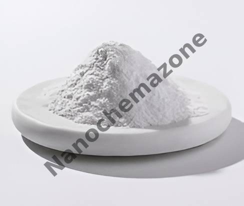
Gold Au Nanoparticles/ Nanopowder AuNPs 99.9%, 20nm

Price range: $245.00 through $430.00
Select options This product has multiple variants. The options may be chosen on the product page
$245/0.5g $430/1g

Product 

Gold Au Nanoparticles/ Nanopowder AuNPs 99.9%, 20nm

CAS No.

7440-57-5

Appearance

Powder

Purity

≥99%,  ≥99.9%,  ≥95%

(Other purities are also available)

APS

20nm (Size Can be customized), Ask for other available size ranges.

Ingredient

AlN

Molecular Weight

196.966 g/mol

Melting Point

1063-1064°C

Boiling Point

2808 °C

Density

19.32 g/cm³

Product Codes

NCZ-1017K

Platinum Nanopowder/Nanoparticles (Pt, 99.9%, ~20nm)

Price range: $245.00 through $430.00
Select options This product has multiple variants. The options may be chosen on the product page
$245/0.5g
$430/1g

Product 

Platinum Nanopowder/Nanoparticles (Pt, 99.9%, ~20nm)

CAS No.

7440-06-4

Appearance

Powder

Purity

≥99%,  ≥99.9%,  ≥95%

(Other purities are also available)

APS

20nm (Size Can be customized), Ask for other available size ranges.

Ingredient

N/A

Molecular Weight

195.08 g/mol

Melting Point

1,768 °C

Boiling Point

 3,825 °C

Density

~21.45 g/cm³

Product Codes

NCZ-1062K