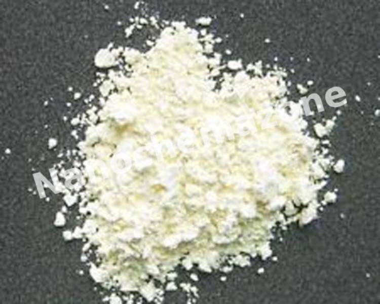
Aluminum (Al) Sputtering Targets, Purity: 99.999%, Size: 6”, Thickness: 0.125”

$213.00

 Applications of Sputtering Targets;

  • Sputtering targets is used for film deposition. The deposition made by sputter targets is a method of depositing thin films by sputtering that involves eroding material from a "target" source onto a "substrate" such as  a silicon wafer.
  • Semiconductor sputtering targets is used to etch the target. Sputter etching is chosen in cases where a high degree of etching anisotropy is needed and selectivity is not a concern.
  • Sputter targets is also used for analysis by etching away the target material.
One of the example occurs in secondary ion spectroscopy (SIMS), where the target sample is sputtered at a constant rate. As the target is sputtered, the concentration and identity of sputtered atoms are measured using mass spectrometry. By helping of the sputtering target, the composition of the target material can be determined and even extremely low concentrations of impurities are detected. Sputtering target has also application area in space. Sputtering is one of the forms of space weathering, a process that changes the physical and chemical properties of airless bodies, such as asteroids and the Moon. Aluminum which has the chemical symbol of Al, is a silvery white, soft, ductile metal that is the third most abundant element. Aluminum is notable due to for its light weight, strength, durability and for its ability to resist corrosion. Aluminum forms an extremely thin but very strong layer of oxide film. Aluminum has also high thermal and electrical conductivity. Aluminum sputtering targets have a particularly fine-grained microstructure. This property of Aluminum sputtering targets ensures that you benefit from uniform erosion and a low susceptibility to particle formation throughout the sputtering process.

Silicon Dioxide (SiO2) Sputtering Targets, Fused Quartz, Purity: 99.995%, Size: 5”, Thickness: 0.250”

$213.00

Applications of Sputtering Targets;

Film deposition is accomplished using sputtering targets. A technique for sputtering thin films is called "deposition made by sputter targets," which entails eroding material from a "target" source onto a "substrate" like a silicon wafer. Etching of the target is done using semiconductor sputtering targets. When selectivity is not an issue and a high degree of etching anisotropy is required, sputter etching is the method of choice. By removing the target material through etching, sputter targets are also utilized for investigation. In secondary ion spectroscopy (SIMS), one example is when the target material is sputtered at a steady pace. Mass spectrometry is used to quantify the concentration and identity of spewed atoms as the target is sputtered.

The target material's composition may be ascertained and even very low concentrations of contaminants can be found with the aid of the sputtering target.

There is also an application area for sputtering targets in space. One type of space weathering that alters the chemical and physical characteristics of airless worlds like the Moon and asteroids is sputtering.

Antimony Sputtering Target (Sb)

Price range: $213.00 through $453.00
Select options This product has multiple variants. The options may be chosen on the product page
Product Antimony Sputtering Target (Sb)
CAS No. 7440-36-0
Appearance Silvery, Lustrous Gray, Semi-metallic
Purity ≥99%,  ≥99.9%,  ≥95%(Other purities are also available)
APS N/A
Ingredient Sb
Molecular Weight 121.76 g/mol
Melting Point 630 °C
Boiling Point 17500 °C
Density N/A
Product Codes NCZ-103H
 

1g Amine Functionalized Graphene Oxide Powder

$213.00
Product 1g Amine Functionalized Graphene Oxide Powder
CAS No. 7782-42-5
Appearance Black
Purity ≥99%,  ≥99.9%,  ≥95%(Other purities are also available)
APS 0.5–5µm (Size Can be customized),  Ask for other available size range.
Ingredient CₓHᵧONₙ
Molecular Weight 79.87 g/mol
Melting Point N/A
Boiling Point N/A
Density 0.0993 g/cm³
Product Codes NCZ-137I

1g Reduced Monolayer Graphene Oxide

$213.00
Product 1g Reduced Monolayer Graphene Oxide
CAS No. 7782-42-5
Appearance Black or dark gray
Purity ≥99%,  ≥99.9%,  ≥95%(Other purities are also available)
APS 0.5–10µmnm (Size Can be customized),  Ask for other available size range.
Ingredient C₁₀H₂O₁
Molecular Weight N/A
Melting Point 300°C
Boiling Point N/A
Density 1.8 – 2.2 g/cm³
Product Codes NCZ-141I
 

Aluminum (Al) Sputtering Targets, Purity: 99.99%, Size: 4”, Thickness: 0.250”

$213.00

Product 

Aluminum (Al) Sputtering Targets, Purity: 99.99%, Size: 4'', Thickness: 0.250''

CAS No.

 7429-90-5

Appearance

Powder

Purity

≥99%,  ≥99.9%,  ≥95%

(Other purities are also available)

APS

N/A (Size Can be customized), Ask for other available size ranges.

Ingredient

N/A

Molecular Weight

 26.98 g/mol

Melting Point

 660.3 °C

Boiling Point

 2519 °C

Density

 2.70 g/cm³

Product Codes

NCZ-2572K

Erbium Oxide (Er2O3) Sputtering Targets, Purity: 99.99%, Size: 1”, Thickness: 0.250”

$214.00
Select options This product has multiple variants. The options may be chosen on the product page

Applications of Sputtering Targets;

  • Sputtering targets is used for film deposition. The deposition made by sputter targets is a method of depositing thin films by sputtering that involves eroding material from a "target" source onto a "substrate" such as  a silicon wafer.
  • Semiconductor sputtering targets is used to etch the target. Sputter etching is chosen in cases where a high degree of etching anisotropy is needed and selectivity is not a concern.
  • Sputter targets is also used for analysis by etching away the target material.
One of the example occurs in secondary ion spectroscopy (SIMS), where the target sample is sputtered at a constant rate. As the target is sputtered, the concentration and identity of sputtered atoms are measured using mass spectrometry. By helping of the sputtering target, the composition of the target material can be determined and even extremely low concentrations of impurities are detected. Sputtering target has also application area in space. Sputtering is one of the forms of space weathering, a process that changes the physical and chemical properties of airless bodies, such as asteroids and the Moon. Erbium oxide with a chemical formula of Er2Ois an oxide of erbium metal. The applications of erbium oxide are varied due to their electrical, optical and photoluminescence properties. Nanoscale materials doped with Er+3 are of much interest because they have special particle-size-dependent optical and electrical properties. Erbium oxide doped nanoparticle materials can be dispersed in glass or plastic for display purposes, such as display monitors. The spectroscopy of Er+3 electronic transitions in host crystals lattices of nanoparticles combined with ultrasonically formed geometries in aqueous solution of carbon nanotubes is of great interest for synthesis of photoluminescence nanoparticles in ‘green’ chemistry. Erbium oxide is among the most important rare earth metals used in biomedicine. Erbium oxides are also used as gate dielectrics in semiconductor devices since it has a high dielectric constant (10-14) and a large band gap. Erbium is sometimes used as a coloring for glasses and erbium oxide can also be used as a burnable neutron poison for nuclear fuel. Erbium oxide films obtained by sputtering can be used for their photoluminescence effect.

Copper (Cu) Sputtering Targets, Purity: 99.999%, Size: 3”, Thickness: 0.250”

$214.00

Applications of Sputtering Targets;

Film deposition is accomplished using sputtering targets. A technique for sputtering thin films is called "deposition made by sputter targets," which entails eroding material from a "target" source onto a "substrate" like a silicon wafer. Etching of the target is done using semiconductor sputtering targets. When selectivity is not an issue and a high degree of etching anisotropy is required, sputter etching is the method of choice. By removing the target material through etching, sputter targets are also utilized for investigation. In secondary ion spectroscopy (SIMS), one example is when the target material is sputtered at a steady pace. Mass spectrometry is used to quantify the concentration and identity of spewed atoms as the target is sputtered.

The target material's composition may be ascertained and even very low concentrations of contaminants can be found with the aid of the sputtering target.

There is also an application area for sputtering targets in space. One type of space weathering that alters the chemical and physical characteristics of airless worlds like the Moon and asteroids is sputtering.

Erbium Oxide (Er2O3) Sputtering Targets, Purity: 99.99%, Size: 1”, Thickness: 0.250”

$214.00

Applications of Sputtering Targets;

Film deposition is accomplished using sputtering targets. A technique for sputtering thin films is called "deposition made by sputter targets," which entails eroding material from a "target" source onto a "substrate" like a silicon wafer. Etching of the target is done using semiconductor sputtering targets. When selectivity is not an issue and a high degree of etching anisotropy is required, sputter etching is the method of choice. By removing the target material through etching, sputter targets are also utilized for investigation. In secondary ion spectroscopy (SIMS), one example is when the target material is sputtered at a steady pace. Mass spectrometry is used to quantify the concentration and identity of spewed atoms as the target is sputtered.

The target material's composition may be ascertained and even very low concentrations of contaminants can be found with the aid of the sputtering target.

There is also an application area for sputtering targets in space. One type of space weathering that alters the chemical and physical characteristics of airless worlds like the Moon and asteroids is sputtering.

Molybdenum Oxide (MoO3) Sputtering Targets, Purity: 99.9%, Size: 1”, Thickness: 0.125”

$214.00

Applications of Sputtering Targets;

Film deposition is accomplished using sputtering targets. A technique for sputtering thin films is called "deposition made by sputter targets," which entails eroding material from a "target" source onto a "substrate" like a silicon wafer. Etching of the target is done using semiconductor sputtering targets. When selectivity is not an issue and a high degree of etching anisotropy is required, sputter etching is the method of choice. By removing the target material through etching, sputter targets are also utilized for investigation. In secondary ion spectroscopy (SIMS), one example is when the target material is sputtered at a steady pace. Mass spectrometry is used to quantify the concentration and identity of spewed atoms as the target is sputtered.

By helping of the sputtering target, the composition of the target material may be evaluated and even extremely tiny amounts of contaminants are recognized.

There is also an application area for sputtering targets in space. One type of space weathering that alters the chemical and physical characteristics of airless worlds like the Moon and asteroids is sputtering.

(-COOH) Functionalized Short Length Single Walled Carbon Nanotubes, Purity: > 92%

Price range: $215.00 through $3,837.00
Select options This product has multiple variants. The options may be chosen on the product page

Applications:

Single Walled Carbon Nanotubes have a variety of potential applications in different fields. These applications include medicine, mechanics, electric-electronics, chemicals, energy and others. It can be applied in, 1-drug delivery, 2-biosensors, 3-CNT composites, 4-catalysis, 5-nanoprobes, 6-hydrogen storage, 7-lithium batteries, 8-gas-discharge tubes, 9-flat panel displays, 10-supercapacitors, 11-transistors, 12-solar cells, 13-photoluminescence, 14-templates

Boron Doped Graphene Nanopowder (B/C)

Price range: $215.00 through $1,413.00
Select options This product has multiple variants. The options may be chosen on the product page

1 gram: 196€

5 grams: 785 €

10 grams: 1284 €

Contact us for larger quantities and other inquires

Boron Doped Graphene

Boron-doped Graphene (BG) is a novel nanomaterial based on graphene, a single sheet of carbon atoms in a hexagonal lattice. The addition of boron atom impurities into pure graphene increases the activation region on its surface, enhances its catalytic ability, accelerates redox reactions, and opens the band gap, giving it numerous applications in fuel cell chemistry, semiconductor devices, ultracapacitors, sensors, and other technologies. Nanografi also manufactures nitrogen-doped graphene and boron/nitrogen co-doped graphene. Please request a quote above to receive pricing information based on your specifications.

DESCRIPTION

  • Typical thickness: <10 layers.
  • Typical size : 5-10 μm.
  • Application
  • Electro catalyst.
  • Field-effect transistors.
  • Sensors.
  • Lithium ion batteries.
  • Supercapacitors.
Compound Formula B/C
Size Range < 10 layers
Average Particle Size 5-10 µm
Morphology Platelets
Thickness 5 nm

Applications

  • 2D Materials
  • Energy Storage & Batteries
  • Fuel Cells
  • Nanomaterials Research
  • Semiconductors

XRD Analysis

XPS Analysis

             Peaks Peak Position (eV) Atomic Contentration (%)
B1s 195,98 11,1
C1s 293,48 77,52
O1s 540,88 11,38

TEM

SEM

Carbon (C) (Graphite) Sputtering Targets, Purity: 99.999%, Size: 4”, Thickness: 0.125”

$215.00

Applications of Sputtering Targets;

Film deposition is accomplished using sputtering targets. A technique for sputtering thin films is called "deposition made by sputter targets," which entails eroding material from a "target" source onto a "substrate" like a silicon wafer. Etching of the target is done using semiconductor sputtering targets. When selectivity is not an issue and a high degree of etching anisotropy is required, sputter etching is the method of choice. By removing the target material through etching, sputter targets are also utilized for investigation. In secondary ion spectroscopy (SIMS), one example is when the target material is sputtered at a steady pace. Mass spectrometry is used to quantify the concentration and identity of spewed atoms as the target is sputtered.

The target material's composition may be ascertained and even very low concentrations of contaminants can be found with the aid of the sputtering target.

There is also an application area for sputtering targets in space. One type of space weathering that alters the chemical and physical characteristics of airless worlds like the Moon and asteroids is sputtering.

Samarium Oxide Nanopowder/ Nanoparticles (Sm2O3, 99.9%, 100nm)

$215.00
Select options This product has multiple variants. The options may be chosen on the product page
$215/25g
Product Samarium Oxide Nanopowder/ Nanoparticles (Sm2O3, 99.9%, 100nm)
CAS No. 12060-58-1
Appearance Yellow to white powder
Purity ≥99%,  ≥99.9%,  ≥95%(Other purities are also available)
APS 100nm (Size Can be customized),  Ask for other available size range.
Ingredient Sm₂O₃. 
Molecular Weight 348.72 g/mol
Melting Point 2,335° C
Boiling Point 4,118° C
Density 8.347g/cm3
Product Codes NCZ-120R
 

Zinc (Zn) Sputtering Targets, Purity: 99.99%, Size: 4”, Thickness: 0.125”

$215.00

Product 

Zinc (Zn) Sputtering Targets, Purity: 99.99%, Size: 4'', Thickness: 0.125''

CAS No.

7440‑66‑6

Appearance

Powder

Purity

≥99%,  ≥99.9%,  ≥95%

(Other purities are also available)

APS

Zn (black granules) (Size Can be customized), Ask for other available size ranges.

Ingredient

N/A

Molecular Weight

65.38 g/mol

Melting Point

419.5 °C

Boiling Point

 907 °C

Density

7.14 g/cm³

Product Codes

NCZ-1467K

Zinc (Zn) Sputtering Targets, Purity: 99.95%, Size: 3”, Thickness: 0.250”

$215.00

Product 

Zinc (Zn) Sputtering Targets, Purity: 99.95%, Size: 3'', Thickness: 0.250''

CAS No.

7440‑66‑6

Appearance

Powder

Purity

≥99%,  ≥99.9%,  ≥95%

(Other purities are also available)

APS

Zn (black granules) (Size Can be customized), Ask for other available size ranges.

Ingredient

N/A

Molecular Weight

65.38 g/mol

Melting Point

419.5 °C

Boiling Point

 907 °C

Density

7.14 g/cm³

Product Codes

NCZ-1468K

Silicon Dioxide (SiO2) Sputtering Targets, Fused Quartz, Purity: 99.995%, Size: 4”, Thickness: 0.125”

$215.00

Product 

Silicon Dioxide (SiO2) Sputtering Targets, Fused Quartz, Purity: 99.995%, Size: 4'', Thickness: 0.125''

CAS No.

7631-86-9

Appearance

Powder

Purity

≥99%,  ≥99.9%,  ≥95%

(Other purities are also available)

APS

N/A  (Size Can be customized), Ask for other available size ranges.

Ingredient

N/A

Molecular Weight

60.08 g/mol

Melting Point

~1710°C

Boiling Point

 ~2,950 °C

Density

~2.20 g/cm³

Product Codes

NCZ-1714K

Nickel Chromium (Ni-Cr) Sputtering Targets, Purity: 99.9%, Size: 2”, Thickness: 0.125”

$215.00

Product 

Nickel Chromium (Ni-Cr) Sputtering Targets, Purity: 99.9%, Size: 2'', Thickness: 0.125''

CAS No.

 11106-97-1

Appearance

Powder

Purity

≥99%,  ≥99.9%,  ≥95%

(Other purities are also available)

APS

 N/A (Size Can be customized), Ask for other available size ranges.

Ingredient

N/A

Molecular Weight

 ~110.69 g/mol

Melting Point

 ~1,400 °C

Boiling Point

 ~2,730–2,750 °C

Density

 ~8.4 – 8.5 g/cm³

Product Codes

NCZ-1859K

Standard pH 10.01 Buffer Powder, 100 Sachets

$215.00
Product Standard pH 10.01 Buffer Powder, 100 Sachets
CAS No. N/A
Appearance White to off-white crystalline
Purity ≥99%,  ≥99.9%,  ≥95%(Other purities are also available)
APS 10–100µm (Size Can be customized),  Ask for other available size range.
Ingredient Na₂B₄O₇·10H₂O
Molecular Weight 40.00 g/mol
Melting Point N/A
Boiling Point N/A
Density 1.2–1.4 g/cm³
Product Codes NCZ-533I

Standard pH 4.01 Buffer Powder, 100 Sachets

$215.00
Product Standard pH 4.01 Buffer Powder, 100 Sachets
CAS No. N/A
Appearance White to off-white crystalline
Purity ≥99%,  ≥99.9%,  ≥95%(Other purities are also available)
APS 10–100µm (Size Can be customized),  Ask for other available size range.
Ingredient KHC₈H₄O₄
Molecular Weight N/A
Melting Point N/A
Boiling Point N/A
Density 1.2–1.4 g/cm³
Product Codes NCZ-535I

Standard pH 7.00 Buffer Powder, 100 Sachets

$215.00
Product Standard pH 7.00 Buffer Powder, 100 Sachets
CAS No. 7778-77-0
Appearance White to off-white fine crystalline
Purity ≥99%,  ≥99.9%,  ≥95%(Other purities are also available)
APS 10–100µm (Size Can be customized),  Ask for other available size range.
Ingredient KH₂PO₄
Molecular Weight 136.09 g/mol
Melting Point N/A
Boiling Point N/A
Density 1.2–1.4 g/cm³
Product Codes NCZ-538I
 

Erbium Oxide (Er2O3) Sputtering Targets, Purity: 99.99%, Size: 4”, Thickness: 0.250”

$215.00

Product 

Erbium Oxide (Er2O3) Sputtering Targets, Purity: 99.99%, Size: 4'', Thickness: 0.250''

CAS No.

12061-16-4

Appearance

Powder

Purity

≥99%,  ≥99.9%,  ≥95%

(Other purities are also available)

APS

 N/A (Size Can be customized), Ask for other available size ranges.

Ingredient

N/A

Molecular Weight

382.52 g/mol

Melting Point

~2,343 °C

Boiling Point

N/A

Density

~8.64 g/cm³

Product Codes

NCZ-2243K

Zinc (Zn) Sputtering Targets, Purity: 99.95%, Size: 6”, Thickness: 0.250”

$216.00

Applications of Sputtering Targets;

Film deposition is accomplished using sputtering targets. A technique for sputtering thin films is called "deposition made by sputter targets," which entails eroding material from a "target" source onto a "substrate" like a silicon wafer. Etching of the target is done using semiconductor sputtering targets. When selectivity is not an issue and a high degree of etching anisotropy is required, sputter etching is the method of choice. By removing the target material through etching, sputter targets are also utilized for investigation. In secondary ion spectroscopy (SIMS), one example is when the target material is sputtered at a steady pace. Mass spectrometry is used to quantify the concentration and identity of spewed atoms as the target is sputtered.

The target material's composition may be ascertained and even very low concentrations of contaminants can be found with the aid of the sputtering target.

There is also an application area for sputtering targets in space. One type of space weathering that alters the chemical and physical characteristics of airless worlds like the Moon and asteroids is sputtering.

3N (99.9%) 300nm Silicon (Si) Nanoparticle Water Dispersion, 5%

Price range: $216.00 through $403.00
Select options This product has multiple variants. The options may be chosen on the product page
Product 3N (99.9%) 300nm Silicon (Si) Nanoparticle Water Dispersion, 5%
CAS No. 7440-21-3
Appearance Grayish-white to light brown
Purity ≥99%,  ≥99.9%,  ≥95%(Other purities are also available)
APS 300nm (Size Can be customized), Ask for other available size range.
Ingredient Si
Molecular Weight 28.0855 g/mol
Melting Point N/A
Boiling Point N/A
Density 2.33 g/cm³
Product Codes NCZ-158I

Carboxylic Double-walled Carbon Nanotubes, 1g

Price range: $216.00 through $286.00
Select options This product has multiple variants. The options may be chosen on the product page
Product Carboxylic Double-walled Carbon Nanotubes, 1g
CAS No. 308068-56-6
Appearance Black fibrous
Purity ≥99%,  ≥99.9%,  ≥95%(Other purities are also available)
APS N/A
Ingredient CₓHᵧO_z
Molecular Weight N/A
Melting Point N/A
Boiling Point N/A
Density 2.1–2.2 g/cm³
Product Codes NCZ-309I

Zinc laurate(Cosmetic grade) (436614)

$216.00
Select options This product has multiple variants. The options may be chosen on the product page
Zinc laurate(Cosmetic grade) (436614)
Product name: Zinc laurate Molecular formula: [CH3(CH2)10COO]2Zn Properties: fine white powder, soluble in hot water and hot ethyl alcohol; lightly soluble in cold ethyl alcohol, ether and other organic solvent   Quality standard
Testing item Testing standard
appearance white fine powder
loss on drying, % ≤1.0
zinc oxide content, % 17.0~19.0
melting point, ℃ 125~135
free acid, % ≤2.0
iodine value ≤1.0
fineness, % 325 mesh passing≥99.0
heavy metal(in Pb), % ≤0.0020
lead, % ≤0.0010
arsenic, % ≤0.0005
Product Codes- NCZ-2713K

Fullerene-C70, Purity: 99%

Price range: $217.00 through $1,052.00
Select options This product has multiple variants. The options may be chosen on the product page
1 gram/194 € 5 grams/940 €                           
Please contact us for quotes on larger quantities !!!

Fullerene-C70

Purity: 99% 

Technical Properties:

Fullerene Compound Formula C70
Fullerene  Molecular Weight 840.77 g/mol
Fullerene  Purity 99%
Fullerene  Melting Point >280 °C
Fullerene  Appearance Black Powder
Fullerene  CAS 115383-22-7

Applications:

1. Pharmaceutical: Diagnostic reagents, super drugs, cosmetics, nuclear magnetic resonance (NMR) with the developer. DNA affinity 2. Energy: Solar battery, fuel cell, secondary battery. 3. Industry: Wear resistant material, flame retardant materials, lubricants, polymer additives, high-performance membrane, catalyst, artificial diamond, hard alloy, electric viscous fluid, ink filters, high-performance coatings, fire retardant coatings, manufacturing bioactive materials , memory materials, embedded molecular and other characteristics, composite materials etc. 4. Information industry: Semiconductor record medium, magnetic materials, printing ink, toner, ink, paper special purposes. 5. Electronic parts: Superconducting semiconductor, diodes, transistors, inductor.  , 6. Optical materials, electronic camera, fluorescence display tube, nonlinear optical materials. 7. Environment: Gas adsorption, gas storage.

Barium (Ba) Sputtering Targets, Purity: 99.5%, Size: 1”, Thickness: 0.250′

$217.00

Applications of Sputtering Targets;

Film deposition is accomplished using sputtering targets. A technique for sputtering thin films is called "deposition made by sputter targets," which entails eroding material from a "target" source onto a "substrate" like a silicon wafer. Etching of the target is done using semiconductor sputtering targets. When selectivity is not an issue and a high degree of etching anisotropy is required, sputter etching is the method of choice. By removing the target material through etching, sputter targets are also utilized for investigation. In secondary ion spectroscopy (SIMS), one example is when the target material is sputtered at a steady pace. When the target shatters,

Mass spectrometry measures the concentration and identity of sputtered atoms. The target material's composition may be ascertained and even very low concentrations of contaminants can be found with the aid of the sputtering target.

There is also an application area for sputtering targets in space. One type of space weathering that alters the chemical and physical characteristics of airless worlds like the Moon and asteroids is sputtering.

A Block S, Group 2, Period 6 element with an atomic weight of 137.27, barium has the atomic symbol Ba and atomic number 56. One of the alkaline-earth metals is barium. Electronics can be plated using barium sputtering targets. Barium has favorable electrical characteristics.

Barium (Ba) Sputtering Targets, Purity: 99.5%, Size: 1”, Thickness: 0.125”

$217.00

Applications of Sputtering Targets;

Film deposition is accomplished using sputtering targets. A technique for sputtering thin films is called "deposition made by sputter targets," which entails eroding material from a "target" source onto a "substrate" like a silicon wafer. Etching of the target is done using semiconductor sputtering targets. When selectivity is not an issue and a high degree of etching anisotropy is required, sputter etching is the method of choice. By removing the target material through etching, sputter targets are also utilized for investigation. In secondary ion spectroscopy (SIMS), one example is when the target material is sputtered at a steady pace. Mass spectrometry is used to quantify the concentration and identity of spewed atoms as the target is sputtered. With the sputtering target's assistance, the

It is possible to identify the target material and even detect incredibly tiny impurity amounts.

There is also an application area for sputtering targets in space. One type of space weathering that alters the chemical and physical characteristics of airless worlds like the Moon and asteroids is sputtering.

A Block S, Group 2, Period 6 element with an atomic weight of 137.27, barium has the atomic symbol Ba and atomic number 56. One of the alkaline-earth metals is barium. Electronics can be plated using barium sputtering targets. Barium has favorable electrical characteristics.

Nickel (Ni) Sputtering Targets, Purity: 99.99%, Size: 3”, Thickness: 0.250”

$217.00

Applications of Sputtering Targets;

Film deposition is accomplished using sputtering targets. A technique for sputtering thin films is called "deposition made by sputter targets," which entails eroding material from a "target" source onto a "substrate" like a silicon wafer. Etching of the target is done using semiconductor sputtering targets. When selectivity is not an issue and a high degree of etching anisotropy is required, sputter etching is the method of choice. By removing the target material through etching, sputter targets are also utilized for investigation. In secondary ion spectroscopy (SIMS), one example is when the target material is sputtered at a steady pace. Mass spectrometry is used to quantify the concentration and identity of spewed atoms as the target is sputtered.

By helping of the sputtering target, the composition of the target material may be evaluated and even extremely tiny amounts of contaminants are recognized.

There is also an application area for sputtering targets in space. One type of space weathering that alters the chemical and physical characteristics of airless worlds like the Moon and asteroids is sputtering.

Zinc Oxide with Alumina (ZnO/Al2O3) Sputtering Target

Price range: $217.00 through $727.00
Select options This product has multiple variants. The options may be chosen on the product page

Product 

Zinc Oxide with Alumina (ZnO/Al2O3) Sputtering Target

CAS No.

1314-13-2 (ZnO) / 1344-28-1 (Al₂O₃)

Appearance

Powder

Purity

≥99%,  ≥99.9%,  ≥95%

(Other purities are also available)

APS

 NA (Size Can be customized), Ask for other available size ranges.

Ingredient

N/A

Molecular Weight

81–90 g/mol

Melting Point

~1,975 °C (ZnO), ~2,050 °C (Al₂O₃)

Boiling Point

N/A

Density

~5.6 g/cm³

Product Codes

NCZ-1332K

Silicon (Si) Sputtering Targets, undoped, Purity: 99.999%, Size: 2”, Thickness: 0.250”

$217.00

Product 

Silicon (Si) Sputtering Targets, undoped, Purity: 99.999%, Size: 2'', Thickness: 0.250''

CAS No.

7440-21-3

Appearance

Powder

Purity

≥99%,  ≥99.9%,  ≥95%

(Other purities are also available)

APS

N/A  (Size Can be customized), Ask for other available size ranges.

Ingredient

N/A

Molecular Weight

28.0855 g/mol

Melting Point

1,414 °C

Boiling Point

 3,265 °C

Density

 2.33 g/cm³

Product Codes

NCZ-1734K

Niobium (Nb) Sputtering Targets, Purity: 99.95% pure Ex Ta, Size: 3”, Thickness: 0.250”

$217.00

Product 

Niobium (Nb) Sputtering Targets, Purity: 99.95% pure Ex Ta, Size: 3'', Thickness: 0.250''

CAS No.

7440-03-1

Appearance

Powder

Purity

≥99%,  ≥99.9%,  ≥95%

(Other purities are also available)

APS

N/A (Size Can be customized), Ask for other available size ranges.

Ingredient

N/A

Molecular Weight

92.906 g/mol

Melting Point

 2,468 °C

Boiling Point

 4,744 °C

Density

 8.57 g/cm³

Product Codes

NCZ-1815K

Nickel Vanadium (NiV) Sputtering Targets, Purity: 99.95%, Size: 1”, Thickness: 0.250”

$217.00

Product 

Nickel Vanadium (NiV) Sputtering Targets, Purity: 99.95%, Size: 1'', Thickness: 0.250''

CAS No.

11137-91-4

Appearance

Powder

Purity

≥99%,  ≥99.9%,  ≥95%

(Other purities are also available)

APS

N/A (Size Can be customized), Ask for other available size ranges.

Ingredient

N/A

Molecular Weight

~57.9 g/mol

Melting Point

~1,350–1,450 °C

Boiling Point

N/A

Density

 ~8.5 g/cm³

Product Codes

NCZ-1829K

Magnesium myristate(Cosmetic grade) (437614)

$217.00
Select options This product has multiple variants. The options may be chosen on the product page
Magnesium myristate(Cosmetic grade) (437614)
Product name: Magnesium myristate Molecular formula: [CH3(CH2)12COO]2Mg Properties: Magnesium myristate is fine white crystal powder; soluble in hot water and hot ethyl alcohol; lightly soluble in organic solvent, such as ethyl alcohol and ether; Main uses It is used as emulsifying agent, lubricating agent, surface active agent, dispersing agent in personal-care supply field.   Quality standard
Testing item Testing standard
appearance white fine powder
loss on drying, % ≤6.0
magnesium oxide content, % 8.2~8.9
melting point, ℃ 132~138
free acid, % ≤3.0
iodine value ≤1.0
fineness  , %  200 mesh passing≥99.0
heavy metal(in Pb), % ≤0.0020
lead, % ≤0.0010
arsenic, % ≤0.0005
Product Codes- NCZ-2715K

Polyhydroxylated Fullerene (Fullerenols)/ C60, (-OH) Functionalized, Dispersed in Water, 500 ppm Dry powder

Price range: $218.00 through $2,664.00
Select options This product has multiple variants. The options may be chosen on the product page
25 ml/195 € 100 ml/450 € 500 ml/1580 € 1000 ml/2380 € Please contact us for quotes on larger quantities.

Polyhydroxylated Fullerene (Fullerenols)/ C60

(-OH) Functionalized, Dispersed in Water, 500 ppm Dry powder

The starting material is >98% purity C60 fullerenes. C60 bearing over 40 hydroxyl groups that have higher water solubility (>50 mg/mL). These exist as monodisperse nanoparticles in water, and have a valiant polishing effect. They exhibit superior antioxidant and anti-inflammatory properties.

Applications:

1. Pharmaceutical: Diagnostic reagents, super drugs, cosmetics, nuclear magnetic resonance (NMR) with the developer. DNA affinity, anti-HIV drugs, anti-cancer drugs, chemotherapy drugs, cosmetics additives and scientific research. 2. Energy: Solar battery, fuel cell, secondary battery. 3. Industry: Wear resistant material, flame retardant materials, lubricants, polymer additives, high-performance membrane, catalyst, artificial diamond, hard alloy, electric viscous fluid, ink filters, high-performance coatings, fire retardant coatings, manufacturing bioactive materials , memory materials, embedded molecular and other characteristics, composite materials etc. 4. Information industry: Semiconductor record medium, magnetic materials, printing ink, toner, ink, paper special purposes. 5. Electronic parts: Superconducting semiconductor, diodes, transistors, inductor.  , 6. Optical materials, electronic camera, fluorescence display tube, nonlinear optical materials. 7. Environment: Gas adsorption, gas storage.  

Fullerene-C70, Purity: 98%

Price range: $218.00 through $1,050.00
Select options This product has multiple variants. The options may be chosen on the product page

Applications:

1. Pharmaceutical: Diagnostic reagents, super drugs, cosmetics, nuclear magnetic resonance (NMR) with the developer. DNA affinity 2. Energy: Solar battery, fuel cell, secondary battery. 3. Industry: Wear resistant material, flame retardant materials, lubricants, polymer additives, high-performance membrane, catalyst, artificial diamond, hard alloy, electric viscous fluid, ink filters, high-performance coatings, fire retardant coatings, manufacturing bioactive materials , memory materials, embedded molecular and other characteristics, composite materials etc. 4. Information industry: Semiconductor record medium, magnetic materials, printing ink, toner, ink, paper special purposes. 5. Electronic parts: Superconducting semiconductor, diodes, transistors, inductor.  , 6. Optical materials, electronic camera, fluorescence display tube, nonlinear optical materials. 7. Environment: Gas adsorption, gas storage.

Vanadium (V) Micron Powder Purity: 99.9%, Size: 325 mesh

Price range: $219.00 through $3,697.00
Select options This product has multiple variants. The options may be chosen on the product page
25 grams/195 € 100 grams/545 € 500 grams/1985 € 1000 grams/3280 €  

Gallium Arsenide (GaAs) Wafer, Size: 4”, Thickness: 300± 25 μm, Double Side Polished, EPI-ready

Price range: $219.00 through $4,418.00
Select options This product has multiple variants. The options may be chosen on the product page
1 piece/198 € 5 pieces/935 € 25 pieces/3980 € Please contact us for quotes on larger quantities !!!

Gallium Arsenide (GaAs) Wafer

Size: 4”, Double Side Polished, Thickness: 300± 25 μm, EPI-ready

Technical Properties:

Quality  GaAs
Materials  GaAs
Size (inch)  4”
Thickness (μm)  300± 25
Polished  Double Side
Dopant  Undoped
Orientation  100
Resistivity   1 E8
Mobility  4500
EPD  ≤5000
Growth method  VGF
OF Length  32.5±1
IF Length  18±1

Applications:

Gallium arsenide (GaAs) is a compound of the elements gallium and arsenic. Gallium arsenide (GaAs) is a semiconductor compound. Gallium arsenide (GaAs)  has a high electron velocity and high saturated electron mobility. This makes gallium arsenide (GaAs) components are useful in fast electronic switching applications and at ultra-high radio frequencies. In 1907, the British discovered infrared emmission from gallium arsenide. This was called electroluminescence. Also, gallium arsenide (GaAs) was used as a solar cells in space for the Venera 3 mission in 1965, which is the first known operational use of gallium arsenide (GaAs). Vertical gradient freeze is the most common method to produce GaAs wafers. Mainly used for circuits, electronics and solar cell applications. Carbon, silicon, tellurium and zinc are some of the dopants that are used to modify the characteristics and electrical properties of gallium arsenide wafers. Wafer flatness and surface purity are ensured by highest quality standards. Boron concentration of gallium arsenide wafers highly depend on the production method. Gallium arsenide wafers with adequate electrical resistancy prevent high current induction in the circuit. Mobility of GaAs wafers can be tailored with different doping levels.
  • Gallium arsenide (GaAs) is used in laser diodes.
  • Gallium arsenide (GaAs) is used in solar cells.
  • Gallium arsenide (GaAs) is used in optical windows.
  • Gallium arsenide (GaAs) is used in monolithic microwave integrated circuits.
  • Gallium arsenide (GaAs) is used in microwave frequency integrated circuits.
  • Gallium arsenide (GaAs) is used in infrared light-emitting diodes.
  • Gallium arsenide (GaAs) is useful in barometers.
  • Gallium arsenide (GaAs) is useful in pharmaceuticals and nuclear medicine tests.
  • Gallium arsenide (GaAs) is useful in high temperature thermometers.

Aluminum (Al) Sputtering Targets, Purity: 99.99%, Size: 8”, Thickness: 0.250”

$219.00

 Applications of Sputtering Targets;

  • Sputtering targets is used for film deposition. The deposition made by sputter targets is a method of depositing thin films by sputtering that involves eroding material from a "target" source onto a "substrate" such as  a silicon wafer.
  • Semiconductor sputtering targets is used to etch the target. Sputter etching is chosen in cases where a high degree of etching anisotropy is needed and selectivity is not a concern.
  • Sputter targets is also used for analysis by etching away the target material.
One of the example occurs in secondary ion spectroscopy (SIMS), where the target sample is sputtered at a constant rate. As the target is sputtered, the concentration and identity of sputtered atoms are measured using mass spectrometry. By helping of the sputtering target, the composition of the target material can be determined and even extremely low concentrations of impurities are detected. Sputtering target has also application area in space. Sputtering is one of the forms of space weathering, a process that changes the physical and chemical properties of airless bodies, such as asteroids and the Moon. Aluminum which has the chemical symbol of Al, is a silvery white, soft, ductile metal that is the third most abundant element. Aluminum is notable due to for its light weight, strength, durability and for its ability to resist corrosion. Aluminum forms an extremely thin but very strong layer of oxide film. Aluminum has also high thermal and electrical conductivity. Aluminum sputtering targets have a particularly fine-grained microstructure. This property of Aluminum sputtering targets ensures that you benefit from uniform erosion and a low susceptibility to particle formation throughout the sputtering process.

Lithium Titanate (Li2TiO3) Sputtering Targets, Purity: 99.95%, Size: 1”, Thickness: 0.250”

$219.00

Product 

Lithium Titanate (Li2TiO3) Sputtering Targets, Purity: 99.95%, Size: 1'', Thickness: 0.250''

CAS No.

12031-82-2

Appearance

Powder

Purity

≥99%,  ≥99.9%,  ≥95%

(Other purities are also available)

APS

 N/A (Size Can be customized), Ask for other available size ranges.

Ingredient

N/A

Molecular Weight

109.75 g/mol

Melting Point

Decomposes before melting (~1,200 °C)

Boiling Point

N/A

Density

~3.41 g/cm³

Product Codes

NCZ-2014K

Sodium laurate(Cosmetic grade) (435614)

$219.00
Select options This product has multiple variants. The options may be chosen on the product page
Sodium laurate(Cosmetic grade) (435614)
Product name: Sodium laurate Molecular formula: CH3(CH2)10COONa Properties: fine white powder; soluble in hot water and hot ethyl alcohol; lightly soluble in cold ethyl alcohol, ether and other organic solvent Quality standard
Testing item Testing standard
appearance white fine powder
ethyl alcohol solubility test meet the specification
loss on drying, % ≤6.0
ignition residue(sulfate), % 29.0~32.0
acid value (H+)/(mmol/100g) ≤5.0
iodine value ≤1.0
fineness, % 200 mesh passing≥99.0
heavy metal(in Pb), % ≤0.0020
lead, % ≤0.0010
arsenic, % ≤0.0005
Product Codes- NCZ-2712K

Short Length Double Walled Carbon Nanotubes, Purity: > 65%

Price range: $220.00 through $3,101.00
Select options This product has multiple variants. The options may be chosen on the product page

Applications:

Double Walled Carbon Nanotubes have a variety of potential applications in different fields. These applications include medicine, mechanics, electric-electronics, chemicals, energy and others. It can be applied in, 1-drug delivery, 2-biosensors, 3-CNT composites, 4-catalysis, 5-nanoprobes, 6-hydrogen storage, 7-lithium batteries, 8-gas-discharge tubes, 9-flat panel displays, 10-supercapacitors, 11-transistors, 12-solar cells, 13-photoluminescence, 14-templates

Single Walled Carbon Nanotubes, Purity: > 96%, Dia: 1.0 nm

Price range: $220.00 through $2,807.00
Select options This product has multiple variants. The options may be chosen on the product page

Single Walled Carbon Nanotubes

Purity: > 96%, Dia: 1.0 nm

Single walled carbon nanotubes (SWCNTs, SWNTs) comprise of one-atom-thick sheets of graphene that rolled up to form long hollow tubes. SWCNTs possess exceptional thermal, mechanical and electrical properties. These remarkable properties lead to advances in performance in a wide range of materials and devices. Single-walled carbon nanotubes are actively used in diverse area including energy storage, molecular electronics, nanomechanial devices, composites and bio-sensing. Our Single Wall Carbon Nanotubes compete on price and performance with counterparts.

Graphene Sample Pack (Includes 9 products)

Price range: $220.00 through $605.00
Select options This product has multiple variants. The options may be chosen on the product page

Applications:

 Use as a high performance additive for composites with PPO, POM ,PPS, PC, ABS, PP, PE, PS, Nylon and rubbers.  Can improve composites tensile strength, stiffness, corrosion resistance, abrasion resistance and anti-static electricity and lubricant properties.  For all mechanical properties modifications, typical amounts are about 2-6 wt%  For conductivity modification, typical amounts are about 2-8 wt% The addition of Graphene to different composites show improvements in their physical properties. These improvements include electrical conductivity, thermal conductivity, hardness, strength, viscosity etc. Moreover, graphene can replace materials that are used in today’s applications resulting in enhancement of their applications. For example graphene can be integrated into plastics such as epoxy to create a material that can replace steel in the structure of aircraft, improving fuel efficiency, range and reducing weight. It could even be used to coat aircraft surface material to prevent electrical damage resulting from lightning strikes due to its high conductivity.

Erbium Oxide (Er2O3) Sputtering Targets, Purity: 99.99%, Size: 2”, Thickness: 0.250” €220.00

$220.00
Select options This product has multiple variants. The options may be chosen on the product page

Applications of Sputtering Targets;

  • Sputtering targets is used for film deposition. The deposition made by sputter targets is a method of depositing thin films by sputtering that involves eroding material from a "target" source onto a "substrate" such as  a silicon wafer.
  • Semiconductor sputtering targets is used to etch the target. Sputter etching is chosen in cases where a high degree of etching anisotropy is needed and selectivity is not a concern.
  • Sputter targets is also used for analysis by etching away the target material.
One of the example occurs in secondary ion spectroscopy (SIMS), where the target sample is sputtered at a constant rate. As the target is sputtered, the concentration and identity of sputtered atoms are measured using mass spectrometry. By helping of the sputtering target, the composition of the target material can be determined and even extremely low concentrations of impurities are detected. Sputtering target has also application area in space. Sputtering is one of the forms of space weathering, a process that changes the physical and chemical properties of airless bodies, such as asteroids and the Moon. Erbium oxide with a chemical formula of Er2Ois an oxide of erbium metal. The applications of erbium oxide are varied due to their electrical, optical and photoluminescence properties. Nanoscale materials doped with Er+3 are of much interest because they have special particle-size-dependent optical and electrical properties. Erbium oxide doped nanoparticle materials can be dispersed in glass or plastic for display purposes, such as display monitors. The spectroscopy of Er+3 electronic transitions in host crystals lattices of nanoparticles combined with ultrasonically formed geometries in aqueous solution of carbon nanotubes is of great interest for synthesis of photoluminescence nanoparticles in ‘green’ chemistry. Erbium oxide is among the most important rare earth metals used in biomedicine. Erbium oxides are also used as gate dielectrics in semiconductor devices since it has a high dielectric constant (10-14) and a large band gap. Erbium is sometimes used as a coloring for glasses and erbium oxide can also be used as a burnable neutron poison for nuclear fuel. Erbium oxide films obtained by sputtering can be used for their photoluminescence effect.

Erbium Oxide (Er2O3) Sputtering Targets, Purity: 99.99%, Size: 2”, Thickness: 0.250”

$220.00

Applications of Sputtering Targets;

Film deposition is accomplished using sputtering targets. A technique for sputtering thin films is called "deposition made by sputter targets," which entails eroding material from a "target" source onto a "substrate" like a silicon wafer. Etching of the target is done using semiconductor sputtering targets. When selectivity is not an issue and a high degree of etching anisotropy is required, sputter etching is the method of choice. By removing the target material through etching, sputter targets are also utilized for investigation. In secondary ion spectroscopy (SIMS), one example is when the target material is sputtered at a steady pace. Mass spectrometry is used to quantify the concentration and identity of spewed atoms as the target is sputtered.

The target material's composition may be ascertained and even very low concentrations of contaminants can be found with the aid of the sputtering target.

There is also an application area for sputtering targets in space. One type of space weathering that alters the chemical and physical characteristics of airless worlds like the Moon and asteroids is sputtering.

Magnesium (Mg) Sputtering Targets, Purity: 99.95%, Size: 4”, Thickness: 0.125”

$220.00

Applications of Sputtering Targets;

Film deposition is accomplished using sputtering targets. A technique for sputtering thin films is called "deposition made by sputter targets," which entails eroding material from a "target" source onto a "substrate" like a silicon wafer. Etching of the target is done using semiconductor sputtering targets. When selectivity is not an issue and a high degree of etching anisotropy is required, sputter etching is the method of choice. By removing the target material through etching, sputter targets are also utilized for investigation. In secondary ion spectroscopy (SIMS), one example is when the target material is sputtered at a steady pace. Mass spectrometry is used to quantify the concentration and identity of spewed atoms as the target is sputtered.

By helping of the sputtering target, the composition of the target material may be evaluated and even extremely tiny amounts of contaminants are recognized.

There is also an application area for sputtering targets in space. One type of space weathering that alters the chemical and physical characteristics of airless worlds like the Moon and asteroids is sputtering.

Molybdenum (Mo) Sputtering Targets, Purity: 99.95%, Size: 4”, Thickness: 0.250”

$220.00

Applications of Sputtering Targets;

Film deposition is accomplished using sputtering targets. A technique for sputtering thin films is called "deposition made by sputter targets," which entails eroding material from a "target" source onto a "substrate" like a silicon wafer. Etching of the target is done using semiconductor sputtering targets. When selectivity is not an issue and a high degree of etching anisotropy is required, sputter etching is the method of choice. By removing the target material through etching, sputter targets are also utilized for investigation. In secondary ion spectroscopy (SIMS), one example is when the target material is sputtered at a steady pace. Mass spectrometry is used to quantify the concentration and identity of spewed atoms as the target is sputtered.

By helping of the sputtering target, the composition of the target material may be evaluated and even extremely tiny amounts of contaminants are recognized.

There is also an application area for sputtering targets in space. One type of space weathering that alters the chemical and physical characteristics of airless worlds like the Moon and asteroids is sputtering.

Nickel Chromium (Ni-Cr) Sputtering Targets, Purity: 99.9%, Size: 2”, Thickness: 0.250”

$220.00

Applications of Sputtering Targets;

Film deposition is accomplished using sputtering targets. A technique for sputtering thin films is called "deposition made by sputter targets," which entails eroding material from a "target" source onto a "substrate" like a silicon wafer. Etching of the target is done using semiconductor sputtering targets. When selectivity is not an issue and a high degree of etching anisotropy is required, sputter etching is the method of choice. By removing the target material through etching, sputter targets are also utilized for investigation. In secondary ion spectroscopy (SIMS), one example is when the target material is sputtered at a steady pace. Mass spectrometry is used to quantify the concentration and identity of spewed atoms as the target is sputtered.

The target material's composition may be ascertained and even very low concentrations of contaminants can be found with the aid of the sputtering target.

There is also an application area for sputtering targets in space. One type of space weathering that alters the chemical and physical characteristics of airless worlds like the Moon and asteroids is sputtering.

Nickel Iron (Ni-Fe) Sputtering Targets, Purity: 99.95%, Size: 2”, Thickness: 0.250”

$220.00

Applications of Sputtering Targets;

Film deposition is accomplished using sputtering targets. A technique for sputtering thin films is called "deposition made by sputter targets," which entails eroding material from a "target" source onto a "substrate" like a silicon wafer. Etching of the target is done using semiconductor sputtering targets. When selectivity is not an issue and a high degree of etching anisotropy is required, sputter etching is the method of choice. By removing the target material through etching, sputter targets are also utilized for investigation. In secondary ion spectroscopy (SIMS), one example is when the target material is sputtered at a steady pace. Mass spectrometry is used to quantify the concentration and identity of spewed atoms as the target is sputtered.

The target material's composition may be ascertained and even very low concentrations of contaminants can be found with the aid of the sputtering target.

There is also an application area for sputtering targets in space. One type of space weathering that alters the chemical and physical characteristics of airless worlds like the Moon and asteroids is sputtering.

3N5 (99.95%) Niobium (Nb) Wire (0.5mm Dia.) Evaporation Materials

Price range: $220.00 through $352.00
Select options This product has multiple variants. The options may be chosen on the product page
Product 3N5 (99.95%) Niobium (Nb) Wire (0.5mm Dia.) Evaporation Materials
CAS No. 7440-03-1
Appearance Gray, Metallic
Purity ≥99%,  ≥99.9%,  ≥95%(Other purities are also available)
APS 0.5mm (Size Can be customized),  Ask for other available size range.
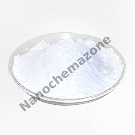
Ingredient Nb
Molecular Weight 92.91 g/mol
Melting Point 2,468 °C
Boiling Point N/A
Density 8.57 g/cm³
Product Codes NCZ-141E

5N 0.3-10 um Alpha Aluminum Oxide (Alumina) Al2O3 Powder, 500 g

$220.00
Product 5N 0.3-10 um Alpha Aluminum Oxide (Alumina) Al2O3 Powder, 500 g
CAS No. 1344-28-1
Appearance White
Purity ≥99%,  ≥99.9%,  ≥95%(Other purities are also available)
APS 0.3-10um (Size Can be customized),  Ask for other available size range.
Ingredient Al2O3
Molecular Weight 101.96 g/mol
Melting Point 1N/A
Boiling Point N/A
Density 0.4-0.6 g/cm3
Product Codes NCZ-256I
 

Carbon Quantum Dot Dispersion (Green Fluorescence)

$220.00
Select options This product has multiple variants. The options may be chosen on the product page
Product Carbon Quantum Dot Dispersion (Green Fluorescence)
CAS No. 7789-75-5
Appearance Clear to pale yellow or brown
Purity ≥99%,  ≥99.9%,  ≥95%(Other purities are also available)
APS 2–10nm (Size Can be customized),  Ask for other available size range.
Ingredient CₓHᵧN_zO_w
Molecular Weight N/A
Melting Point N/A
Boiling Point N/A
Density 1.8–2.2 g/cm³
Product Codes NCZ-303I

Cobalt (Co) Nanopowder/Nanoparticles, Purity: 99.5%, Size: 100 nm

Price range: $221.00 through $1,219.00
Select options This product has multiple variants. The options may be chosen on the product page

Cobalt (Co) Nanopowder/Nanoparticles

Purity: 99.5%, Size: 100 nm

Cobalt is a chemical element with the atomic number 27. Cobalt is found in chemically combined form. The cobalt is hard and solid with grayish color. Cobalt has a high boiling and melting points. At room temperature and standard pressure cobalt can barely be oxidized. But if cobalt is heated, a cobalt oxide is formed. The oxide from cobalt can be used in many useful applications and the material acquires various colors depending on Cobalts oxidation state.

Cobalt (Co) Nanopowder/Nanoparticles, Purity: 99.5%, Size: 100 nm

Price range: $221.00 through $1,220.00
Select options This product has multiple variants. The options may be chosen on the product page
100 grams/195 €                     
500 grams/666 €                    
1000 grams/1074 € Please contact us for quotes on larger quantities !!!

Cobalt (Co) Nanopowder/Nanoparticles

Purity: 99.5%, Size: 100 nm

Cobalt is a chemical element with the atomic number 27. Cobalt is found in chemically combined form. The cobalt is hard and solid with grayish color. Cobalt has a high boiling and melting points. At room temperature and standard pressure cobalt can barely be oxidized. But if cobalt is heated, a cobalt oxide is formed. The oxide from cobalt can be used in many useful applications and the material acquires various colors depending on Cobalts oxidation state.

Aluminum Oxide (Al2O3) Nanopowder/Nanoparticles Dispersion in 2-Propanol, Gamma, Size: 12 nm, 12 wt%

Price range: $221.00 through $1,129.00
Select options This product has multiple variants. The options may be chosen on the product page
120 ml/195 € 500 ml/645 € 1000 ml/994 €      
Please contact us for quotes on larger quantities !!!

Aluminum Oxide (Al2O3) Nanopowder/Nanoparticles Dispersion in 2-Propanol

Gamma, Size: 12 nm, 12 wt%

Cadmium (Cd) Sputtering Target

Price range: $221.00 through $625.00
Select options This product has multiple variants. The options may be chosen on the product page

Product 

Cadmium (Cd) Sputtering Target

CAS No.

7440-43-9

Appearance

Powder

Purity

≥99%,  ≥99.9%,  ≥95%

(Other purities are also available)

APS

 NA (Size Can be customized), Ask for other available size ranges.

Ingredient

N/A

Molecular Weight

112.41 g/mol

Melting Point

321.07 °C

Boiling Point

767 °C

Density

8.65 g/cm³

Product Codes

NCZ-1286K

Zinc (Zn) Sputtering Targets, Purity: 99.95%, Size: 4”, Thickness: 0.125”

$221.00

Product 

Zinc (Zn) Sputtering Targets, Purity: 99.95%, Size: 4'', Thickness: 0.125''

CAS No.

7440‑66‑6

Appearance

Powder

Purity

≥99%,  ≥99.9%,  ≥95%

(Other purities are also available)

APS

Zn (black granules) (Size Can be customized), Ask for other available size ranges.

Ingredient

N/A

Molecular Weight

65.38 g/mol

Melting Point

419.5 °C

Boiling Point

 907 °C

Density

7.14 g/cm³

Product Codes

NCZ-1466K

Boron Doped Graphene Nanopowder (B/C)

Price range: $223.00 through $1,461.00
Select options This product has multiple variants. The options may be chosen on the product page

Boron Doped Graphene

Boron-doped Graphene (BG) is a novel nanomaterial based on graphene, a single sheet of carbon atoms in a hexagonal lattice. The addition of boron atom impurities into pure graphene increases the activation region on its surface, enhances its catalytic ability, accelerates redox reactions, and opens the band gap, giving it numerous applications in fuel cell chemistry, semiconductor devices, ultracapacitors, sensors, and other technologies. Nanografi also manufactures nitrogen-doped graphene and boron/nitrogen co-doped graphene. Please request a quote above to receive pricing information based on your specifications.