3YSZ Zirconium Dioxide Yttria Stabilized Nanoparticles, 30 nm

Price range: $198.00 through $2,189.00
Select options This product has multiple variants. The options may be chosen on the product page
Product 3YSZ Zirconium Dioxide Yttria Stabilized Nanoparticles, 30 nm
CAS No. 7439-89-6
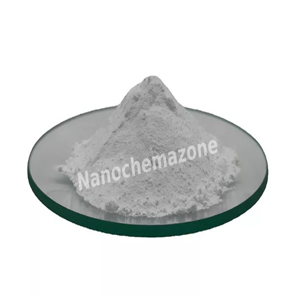
Appearance White or off-white
Purity ≥99%,  ≥99.9%,  ≥95%(Other purities are also available)
APS 30 nm (Size Can be customized),  Ask for other available size range.
Ingredient Fe
Molecular Weight 123.22 g/mol
Melting Point 2,700 °C
Boiling Point N/A
Density 6.0 g/cm³
Product Codes NCZ-162I

3YSZ Zirconium Dioxide Yttria Stabilized Nanoparticles, 50 nm

Price range: $198.00 through $2,189.00
Select options This product has multiple variants. The options may be chosen on the product page
Product 3YSZ Zirconium Dioxide Yttria Stabilized Nanoparticles, 50 nm
CAS No. N/A
Appearance White or off-white
Purity ≥99%,  ≥99.9%,  ≥95%(Other purities are also available)
APS 50nm (Size Can be customized),  Ask for other available size range.
Ingredient (ZrO₂)₀.97·(Y₂O₃)₀.03
Molecular Weight 123.22 g/mol
Melting Point 2,700 °C
Boiling Point N/A
Density N/A
Product Codes NCZ-163I
 

3YSZ Zirconium Oxide Yttria Stabilized Nanoparticles 50nm to 80nm

Price range: $198.00 through $2,185.00
Select options This product has multiple variants. The options may be chosen on the product page
Product 3YSZ Zirconium Oxide Yttria Stabilized Nanoparticles 50nm to 80nm
CAS No. N/A
Appearance White or off-white
Purity ≥99%,  ≥99.9%,  ≥95%(Other purities are also available)
APS 50nm-80nm (Size Can be customized),  Ask for other available size range.
Ingredient (ZrO₂)₀.97·(Y₂O₃)₀.03
Molecular Weight 123.22 g/mol
Melting Point 2,700 °C
Boiling Point N/A
Density 6.0 g/cm³
Product Codes NCZ-164I
 

50-100 um 3YSZ Zirconium Dioxide Yttria Stabilized Powder

Price range: $198.00 through $2,189.00
Select options This product has multiple variants. The options may be chosen on the product page
Product 50-100 um 3YSZ Zirconium Dioxide Yttria Stabilized Powder
CAS No. N/A
Appearance White or off-white
Purity ≥99%,  ≥99.9%,  ≥95%(Other purities are also available)
APS 50-100nm (Size Can be customized),  Ask for other available size range.
Ingredient ZrO₂
Molecular Weight 123.22 g/mol
Melting Point 2,700 °C
Boiling Point N/A
Density 6.05 g/cm³
Product Codes NCZ-185I

5YSZ Zirconium Oxide Yttria Stabilized Nanoparticles 20nm to 40nm

Price range: $198.00 through $2,185.00
Select options This product has multiple variants. The options may be chosen on the product page
Product 5YSZ Zirconium Oxide Yttria Stabilized Nanoparticles 20nm to 40nm
CAS No. 7440-21-3
Appearance White
Purity ≥99%,  ≥99.9%,  ≥95%(Other purities are also available)
APS 20-40nm (Size Can be customized),  Ask for other available size range.
Ingredient (ZrO₂)₀.95(Y₂O₃)₀.05
Molecular Weight N/A
Melting Point N/A
Boiling Point N/A
Density 5.68 g/cm³
Product Codes NCZ-202I
 

Aqueous Conductive Graphene Slurry, 1kg

$198.00
Product Aqueous Conductive Graphene Slurry, 1kg
CAS No. 1034343-98-0
Appearance Black slurry
Purity ≥99%,  ≥99.9%,  ≥95%(Other purities are also available)
APS 4–6µm (Size Can be customized),  Ask for other available size range.
Ingredient CH₂O
Molecular Weight 12.01 g/mol
Melting Point N/A
Boiling Point N/A
Density 1.05–1.20 g/cm³
Product Codes NCZ-289I
 

Molybdenum (Mo) Sputtering Targets, Purity: 99.95%, Size: 3”, Thickness: 0.250”

$198.00

Product 

Molybdenum (Mo) Sputtering Targets, Purity: 99.95%, Size: 3'', Thickness: 0.250''

CAS No.

 7439-98-7

Appearance

Powder

Purity

≥99%,  ≥99.9%,  ≥95%

(Other purities are also available)

APS

 N/A (Size Can be customized), Ask for other available size ranges.

Ingredient

N/A

Molecular Weight

95.95 g/mol

Melting Point

 2623 °C

Boiling Point

 4639 °C

Density

10.28 g/cm³

Product Codes

NCZ-1936K

Holmium Chloride Hexahydrate (HoCl3 · 6H2O) 99.9% 3N

$198.00
Select options This product has multiple variants. The options may be chosen on the product page
Product Holmium Chloride Hexahydrate (HoCl3 · 6H2O) 99.9% 3N
CAS No. 14914-87-1
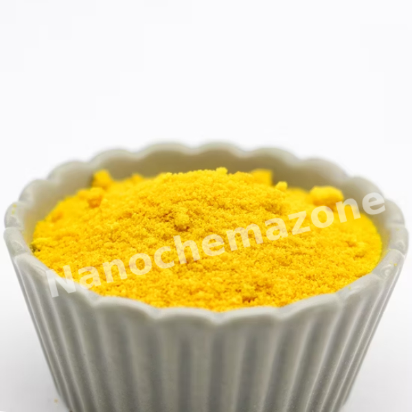
Appearance Pale yellow to pink crystalline
Purity ≥99%,  ≥99.9%,  ≥95%(Other purities are also available)
APS 0–50µm (Size Can be customized),  Ask for other available size range.
Ingredient HoCl3·6H2O
Molecular Weight 379.32 g/mol
Melting Point N/A
Boiling Point N/A
Density 2.6 – 3.0 g/cm³
Product Codes NCZ-419I

Monoclinic Zirconium Oxide (Zirconia) ZrO2 Nanoparticles, 20nm to 40nm, >99.9% High Purity

Price range: $198.00 through $2,185.00
Select options This product has multiple variants. The options may be chosen on the product page
Product Monoclinic Zirconium Oxide (Zirconia) ZrO2 Nanoparticles, 20nm to 40nm, >99.9% High Purity
CAS No. N/A
Appearance White
Purity ≥99%,  ≥99.9%,  ≥95%(Other purities are also available)
APS 20–40nm (Size Can be customized),  Ask for other available size range.
Ingredient ZrO2
Molecular Weight 123.22 g/mol
Melting Point 2,715 °C
Boiling Point N/A
Density 5.68 g/cm³
Product Codes NCZ-454I
 

Monoclinic Zirconium Oxide (Zirconia) ZrO2 Nanoparticles, 50nm to 80nm, >99.9% High Purity

Price range: $198.00 through $2,185.00
Select options This product has multiple variants. The options may be chosen on the product page
Product Monoclinic Zirconium Oxide (Zirconia) ZrO2 Nanoparticles, 50nm to 80nm, >99.9% High Purity
CAS No. 1314-23-4
Appearance White or off-white
Purity ≥99%,  ≥99.9%,  ≥95%(Other purities are also available)
APS 50–80nm (Size Can be customized),  Ask for other available size range.
Ingredient ZrO2
Molecular Weight 123.22 g/mol
Melting Point 2,715 °C
Boiling Point N/A
Density 5.68 g/cm³
Product Codes NCZ-455I

Single Layer Graphene Powder (Chemical Method)

Price range: $198.00 through $396.00
Select options This product has multiple variants. The options may be chosen on the product page
Product Single Layer Graphene Powder (Chemical Method)
CAS No. 7440-44-0
Appearance Black, fine to flaky
Purity ≥99%,  ≥99.9%,  ≥95%(Other purities are also available)
APS 0.5–10µm (Size Can be customized),  Ask for other available size range.
Ingredient C
Molecular Weight N/A
Melting Point N/A
Boiling Point N/A
Density 2.2 g/cm³
Product Codes NCZ-524I
 

Cobalt (Co) Sputtering Targets, Purity: 99.95%, Size: 3”, Thickness: 0.250”

$198.00

Product 

Cobalt (Co) Sputtering Targets, Purity: 99.95%, Size: 3'', Thickness: 0.250''

CAS No.

7440‑48‑4

Appearance

Powder

Purity

≥99%,  ≥99.9%,  ≥95%

(Other purities are also available)

APS

 N/A (Size Can be customized), Ask for other available size ranges.

Ingredient

N/A

Molecular Weight

58.93 g/mol (cobalt atomic weight)

Melting Point

~1,495 °C

Boiling Point

~2,870–2,927 °C

Density

~8.9 g/cm³

Product Codes

NCZ-2290K

Aluminum (Al) Sputtering Targets, Purity: 99.99%, Size: 5”, Thickness: 0.125”

$198.00

Product 

Aluminum (Al) Sputtering Targets, Purity: 99.99%, Size: 5'', Thickness: 0.125''

CAS No.

 7429-90-5

Appearance

Powder

Purity

≥99%,  ≥99.9%,  ≥95%

(Other purities are also available)

APS

N/A (Size Can be customized), Ask for other available size ranges.

Ingredient

N/A

Molecular Weight

 26.98 g/mol

Melting Point

 660.3 °C

Boiling Point

 2519 °C

Density

 2.70 g/cm³

Product Codes

NCZ-2570K

Gallium Arsenide (GaAs) Wafers, Size: 4”, Thickness: 350± 25 μm, Single Side Polished, EPI-ready, Mobility: 1000-3000

Price range: $198.45 through $3,768.00
Select options This product has multiple variants. The options may be chosen on the product page
Gallium Arsenide (GaAs) Wafer Size: 4”, Thickness: 350± 25 μm, Mobility: 1000-3000 Technical Properties: Quality  GaAs Materials  GaAs Size (inch)  4”

Gallium Arsenide (GaAs) Wafers, Size: 4”, Thickness: 625±25 μm, Single Side Polished, EPI-ready

Price range: $198.45 through $3,768.00
Select options This product has multiple variants. The options may be chosen on the product page
Gallium Arsenide (GaAs) Wafer Size: 4”, Thickness: 625±25 μm, Single Side Polished Technical Properties: Quality  GaAs Materials  GaAs Size (inch)

Magnetic Graphene Aerogel, Content of Fe3O4: 50%, Diameter: 1±0.1 cm

Price range: $199.00 through $775.00
Select options This product has multiple variants. The options may be chosen on the product page
Please contact us for quotes for larger quantities !   This aerogel is a self-assembled, 3d porous foam material with high quality sheet layer < 3 graphene oxide and Fe3O4 nanoparticles as raw materials. The aerogel has micron-sized macropores and nano-sized mesoporous pores to form a rich compound void structure. With stable chemical properties, large specific surface area and abundant pores, this aerogel is suitable for the adsorption of copper, chromium, lead and other heavy metals in water.

Carbon (C) (Pyrolytic Graphite) Sputtering Targets, Purity: 99.999%, Size: 1”, Thickness: 0.250”

$199.00

Applications of Sputtering Targets;

Film deposition is accomplished using sputtering targets. A technique for sputtering thin films is called "deposition made by sputter targets," which entails eroding material from a "target" source onto a "substrate" like a silicon wafer. Etching of the target is done using semiconductor sputtering targets. When selectivity is not an issue and a high degree of etching anisotropy is required, sputter etching is the method of choice. By removing the target material through etching, sputter targets are also utilized for investigation. In secondary ion spectroscopy (SIMS), one example is when the target material is sputtered at a steady pace. Mass spectrometry is used to quantify the concentration and identity of spewed atoms as the target is sputtered.

The target material's composition may be ascertained and even very low concentrations of contaminants can be found with the aid of the sputtering target.

There is also an application area for sputtering targets in space. One type of space weathering that alters the chemical and physical characteristics of airless worlds like the Moon and asteroids is sputtering.

Chromium (Cr) Sputtering Targets, Purity: 99.95%, Size: 3”, Thickness: 0.125”

$199.00

Applications of Sputtering Targets;

Film deposition is accomplished using sputtering targets. A technique for sputtering thin films is called "deposition made by sputter targets," which entails eroding material from a "target" source onto a "substrate" like a silicon wafer. Etching of the target is done using semiconductor sputtering targets. When selectivity is not an issue and a high degree of etching anisotropy is required, sputter etching is the method of choice. By removing the target material through etching, sputter targets are also utilized for investigation. In secondary ion spectroscopy (SIMS), one example is when the target material is sputtered at a steady pace. Mass spectrometry is used to quantify the concentration and identity of spewed atoms as the target is sputtered.

The target material's composition may be ascertained and even very low concentrations of contaminants can be found with the aid of the sputtering target.

There is also an application area for sputtering targets in space. One type of space weathering that alters the chemical and physical characteristics of airless worlds like the Moon and asteroids is sputtering.

Silvery, shiny, hard, and brittle, chromium is a metal that resists corrosion and has a high mirror polish. The automotive industry finds extensive use for chromium sputtering targets. Chromium sputtering targets work well as a shiny coating for bumpers and wheels. Chromium sputtering targets can be employed in a variety of vacuum applications, such as automotive glass coatings.

Silver (Ag) Sputtering Targets, Purity: 99.99%, Size: 1”, Thickness: 0.125”

$199.00

Applications of Sputtering Targets;

Film deposition is accomplished using sputtering targets. A technique for sputtering thin films is called "deposition made by sputter targets," which entails eroding material from a "target" source onto a "substrate" like a silicon wafer. Etching of the target is done using semiconductor sputtering targets. When selectivity is not an issue and a high degree of etching anisotropy is required, sputter etching is the method of choice. By removing the target material through etching, sputter targets are also utilized for investigation. In secondary ion spectroscopy (SIMS), one example is when the target material is sputtered at a steady pace. Mass spectrometry is used to quantify the concentration and identity of spewed atoms as the target is sputtered.

The target material's composition may be ascertained and even very low concentrations of contaminants can be found with the aid of the sputtering target.

There is also an application area for sputtering targets in space. One type of space weathering that alters the chemical and physical characteristics of airless worlds like the Moon and asteroids is sputtering.

Zinc Oxide (ZnO) with Alumina Sputtering Targets, Purity: 99.99%, Size: 1”, Thickness: 0.250”

$199.00

Applications of Sputtering Targets;

Film deposition is accomplished using sputtering targets. A technique for sputtering thin films is called "deposition made by sputter targets," which entails eroding material from a "target" source onto a "substrate" like a silicon wafer. Etching of the target is done using semiconductor sputtering targets. When selectivity is not an issue and a high degree of etching anisotropy is required, sputter etching is the method of choice. By removing the target material through etching, sputter targets are also utilized for investigation. In secondary ion spectroscopy (SIMS), one example is when the target material is sputtered at a steady pace. Mass spectrometry is used to quantify the concentration and identity of spewed atoms as the target is sputtered.

The target material's composition may be ascertained and even very low concentrations of contaminants can be found with the aid of the sputtering target.

There is also an application area for sputtering targets in space. One type of space weathering that alters the chemical and physical characteristics of airless worlds like the Moon and asteroids is sputtering.

Silver (Ag) Nanopowder/Nanoparticles Dispersion, Purity: 99.99%, Size: 14 nm, 52000 ppm

Price range: $199.77 through $2,099.81
Select options This product has multiple variants. The options may be chosen on the product page
Silver (Ag) Nanopowder/Nanoparticles Dispersion Purity: 99.99%, Size: 14 nm, 52000 ppm Technical Properties: Ag Nanoparticle Purity (%) 99,99 Ag Concentration (wt%/ppm) 5,0/52000 pH

Magnesium (Mg) Sputtering Targets, Purity: 99.95%, Size: 2”, Thickness: 0.250”

$200.00

Applications of Sputtering Targets;

Film deposition is accomplished using sputtering targets. A technique for sputtering thin films is called "deposition made by sputter targets," which entails eroding material from a "target" source onto a "substrate" like a silicon wafer. Etching of the target is done using semiconductor sputtering targets. When selectivity is not an issue and a high degree of etching anisotropy is required, sputter etching is the method of choice. By removing the target material through etching, sputter targets are also utilized for investigation. In secondary ion spectroscopy (SIMS), one example is when the target material is sputtered at a steady pace. Mass spectrometry is used to quantify the concentration and identity of spewed atoms as the target is sputtered.

By helping of the sputtering target, the composition of the target material may be evaluated and even extremely tiny amounts of contaminants are recognized.

There is also an application area for sputtering targets in space. One type of space weathering that alters the chemical and physical characteristics of airless worlds like the Moon and asteroids is sputtering.

Magnesium (Mg) Sputtering Targets, Purity: 99.95%, Size: 3”, Thickness: 0.125”

$200.00

Applications of Sputtering Targets;

Film deposition is accomplished using sputtering targets. A technique for sputtering thin films is called "deposition made by sputter targets," which entails eroding material from a "target" source onto a "substrate" like a silicon wafer. Etching of the target is done using semiconductor sputtering targets. When selectivity is not an issue and a high degree of etching anisotropy is required, sputter etching is the method of choice. By removing the target material through etching, sputter targets are also utilized for investigation. In secondary ion spectroscopy (SIMS), one example is when the target material is sputtered at a steady pace. Mass spectrometry is used to quantify the concentration and identity of spewed atoms as the target is sputtered.

By helping of the sputtering target, the composition of the target material may be evaluated and even extremely tiny amounts of contaminants are recognized.

There is also an application area for sputtering targets in space. One type of space weathering that alters the chemical and physical characteristics of airless worlds like the Moon and asteroids is sputtering.

Nickel Iron (Ni-Fe) Sputtering Targets, Purity: 99.95%, Size: 2”, Thickness: 0.125”

$200.00

Applications of Sputtering Targets;

Film deposition is accomplished using sputtering targets. A technique for sputtering thin films is called "deposition made by sputter targets," which entails eroding material from a "target" source onto a "substrate" like a silicon wafer. Etching of the target is done using semiconductor sputtering targets. When selectivity is not an issue and a high degree of etching anisotropy is required, sputter etching is the method of choice. By removing the target material through etching, sputter targets are also utilized for investigation. In secondary ion spectroscopy (SIMS), one example is when the target material is sputtered at a steady pace. Mass spectrometry is used to quantify the concentration and identity of spewed atoms as the target is sputtered.

The target material's composition may be ascertained and even very low concentrations of contaminants can be found with the aid of the sputtering target.

There is also an application area for sputtering targets in space. One type of space weathering that alters the chemical and physical characteristics of airless worlds like the Moon and asteroids is sputtering.

Silicon (Si) Sputtering Targets, N-type, Purity: 99.999%, Size: 2”, Thickness: 0.125”

$200.00

Applications of Sputtering Targets;

Film deposition is accomplished using sputtering targets. A technique for sputtering thin films is called "deposition made by sputter targets," which entails eroding material from a "target" source onto a "substrate" like a silicon wafer. Etching of the target is done using semiconductor sputtering targets. When selectivity is not an issue and a high degree of etching anisotropy is required, sputter etching is the method of choice. By removing the target material through etching, sputter targets are also utilized for investigation. In secondary ion spectroscopy (SIMS), one example is when the target material is sputtered at a steady pace. Mass spectrometry is used to quantify the concentration and identity of spewed atoms as the target is sputtered.

The target material's composition may be ascertained and even very low concentrations of contaminants can be found with the aid of the sputtering target.

There is also an application area for sputtering targets in space. One type of space weathering that alters the chemical and physical characteristics of airless worlds like the Moon and asteroids is sputtering.

Silicon (Si) Sputtering Targets, P-type, Purity: 99.999%, Size: 2”, Thickness: 0.125”

$200.00

Applications of Sputtering Targets;

Film deposition is accomplished using sputtering targets. A technique for sputtering thin films is called "deposition made by sputter targets," which entails eroding material from a "target" source onto a "substrate" like a silicon wafer. Etching of the target is done using semiconductor sputtering targets. When selectivity is not an issue and a high degree of etching anisotropy is required, sputter etching is the method of choice. By removing the target material through etching, sputter targets are also utilized for investigation. In secondary ion spectroscopy (SIMS), one example is when the target material is sputtered at a steady pace. Mass spectrometry is used to quantify the concentration and identity of spewed atoms as the target is sputtered.

The target material's composition may be ascertained and even very low concentrations of contaminants can be found with the aid of the sputtering target.

There is also an application area for sputtering targets in space. One type of space weathering that alters the chemical and physical characteristics of airless worlds like the Moon and asteroids is sputtering.

Tungsten (W) Sputtering Targets, Purity: 99.95%, Size: 2”, Thickness: 0.125”

$200.00

Applications of Sputtering Targets;

Film deposition is accomplished using sputtering targets. A technique for sputtering thin films is called "deposition made by sputter targets," which entails eroding material from a "target" source onto a "substrate" like a silicon wafer. Etching of the target is done using semiconductor sputtering targets. When selectivity is not an issue and a high degree of etching anisotropy is required, sputter etching is the method of choice. By removing the target material through etching, sputter targets are also utilized for investigation. In secondary ion spectroscopy (SIMS), one example is when the target material is sputtered at a steady pace. Mass spectrometry is used to quantify the concentration and identity of spewed atoms as the target is sputtered.

The target material's composition may be ascertained and even very low concentrations of contaminants can be found with the aid of the sputtering target.

There is also an application area for sputtering targets in space. One type of space weathering that alters the chemical and physical characteristics of airless worlds like the Moon and asteroids is sputtering.

Zinc (Zn) Sputtering Targets, Purity: 99.99% Size: 3”, Thickness: 0.125”

$200.00

Product 

Zinc (Zn) Sputtering Targets, Purity: 99.99% Size: 3'', Thickness: 0.125''

CAS No.

7440‑66‑6

Appearance

Powder

Purity

≥99%,  ≥99.9%,  ≥95%

(Other purities are also available)

APS

Zn (black granules) (Size Can be customized), Ask for other available size ranges.

Ingredient

N/A

Molecular Weight

65.38 g/mol

Melting Point

419.5 °C

Boiling Point

 907 °C

Density

7.14 g/cm³

Product Codes

NCZ-1471K

Praseodymium (Pr) Sputtering Targets, Purity: 99.9%, Size: 3”, Thickness: 0.125”

$200.00

Product 

Praseodymium (Pr) Sputtering Targets, Purity: 99.9%, Size: 3'', Thickness: 0.125''

CAS No.

7440-10-0

Appearance

Powder

Purity

≥99%,  ≥99.9%,  ≥95%

(Other purities are also available)

APS

N/A (Size Can be customized), Ask for other available size ranges.

Ingredient

N/A

Molecular Weight

 140.91 g/mol

Melting Point

931 °C

Boiling Point

 3520 °C

Density

 6.77 g/cm³

Product Codes

NCZ-1791K

Niobium Oxide (Nb2O5) Sputtering Targets, Purity: 99.5%, Size: 2”, Thickness: 0.125”

$200.00

Product 

Niobium Oxide (Nb2O5) Sputtering Targets, Purity: 99.5%, Size: 2'', Thickness: 0.125''

CAS No.

1313-96-8

Appearance

Powder

Purity

≥99%,  ≥99.9%,  ≥95%

(Other purities are also available)

APS

N/A (Size Can be customized), Ask for other available size ranges.

Ingredient

N/A

Molecular Weight

 265.81 g/mol

Melting Point

~1512 °C

Boiling Point

N/A

Density

 4.6 – 4.9 g/cm³

Product Codes

NCZ-1810K

Poly(DL-lactide-co-glycolide)(PLGA85/15) (631989)

Price range: $200.00 through $1,045.00
Select options This product has multiple variants. The options may be chosen on the product page
Poly(DL-lactide-co-glycolide)(PLGA85/15) (631989)
Grade Inherent viscosity (dL/g) Weight average molecular weight (x10000)
PLGA85/15-02 0.1-0.2 0.7-2
PLGA85/15-04 0.204 2-5
PLGA85/15-06 0.4-0.6 5-7
PLGA85/15-08 0.6-0.8 7-10
PLGA85/15-10 0.8-1 0 10-13
PLGA85/15-12 1.0-1.2 13-20
PLGA85/15-15 1.2 1 5 20-30
Product Codes- NCZ-2637K

Hollow glass microsphere (337620)

$200.00
Hollow glass microsphere (337620) Hollow glass microsphere is a kind of ultra-lightweight inorganic non-metallic material with hollow structure, and it is a versatile and high-performance new lightweight material developed in recent years. Its true density is 0.20-0.60g/cm3 with 2-150μm in diameter. It features light weight, large bulky, low thermal conductivity, high compressive strength, smoothly mobility, etc. It can be used in paint and coatings, rubber, plastics, FRP, artificial stone, putty and other products as filler and weight-reducing agent. Because of its high compressive properties, it can be used to produce high-strength, low-density cement slurry and low-density drilling fluid in oil and gas extraction industry.
  1. Chemical composition
Silica(SiO2) 68-75%
Soda(Na2O) 22-30%
Lime(CaO)
Others 2-3%
  1. True Density
 Product Requirement (g/cm3) True Density (g/cm3)
Minimum Maximum
H20 0.20 0.18 0.22
H25 0.25 0.23 0.27
H32 0.32 0.30 0.34
H38H 0.38 0.36 0.40
H40 0.40 0.38 0.42
H46 0.46 0.44 0.48
H60 0.60 0.57 0.63
Y12000 0.60 0.57 0.63
  1. Nitrogen Isostatic Crush Strength
 Product Test Pressure (MPa/Psi) Target  Fractional Survival Minimum Fractional Survival
H20 3.45/500 90% 80%
H25 5/750 90% 80%
H32 14/2000 90% 80%
H38H 38/5500 90% 80%
H40 28/4000 90% 80%
H46 41/6000 90% 80%
H60 55/8000 90% 80%
Y12000 82/12000 90% 80%
  1. Thermal Stability
Appreciable changes in glass microspheres properties may occur above 600°C depending on temperature and duration of exposure.
  1. Chemical Resistance
In general, the chemical properties of hollow glass microspheres resemble those of a soda-lime borosilicate glass.
  1. Thermal Conductivity
 Product Thermal Conductivity (W·m-1·K-1) at 20°C
H20 0.039
H25 0.045
H32 0.050
H38H 0.054
H40 0.056
H46 0.062
H60 0.074
Y12000 0.078
  1. Flotation
 Product  Floaters (% by bulk volume)
Typical Minimum
H20 96% 93%
H25 96% 93%
H32 96% 92%
H38H 95% 92%
H40 95% 92%
H46 95% 92%
H60 95% 92%
Y12000 95% 92%
  1. Oil Absorption
0.45-0.65g oil/cm3 of hollow glass microspheres.
  1. Particle Size
 Product Particle Size(μm, by volume)
10% 50% 90% d50 Size
H20 35 65 120 68 2-150
H25 30 60 115 60 2-150
H32 25 55 105 55 2-130
H38H 22 40 70 40 2-100
H40 25 50 90 48 2-100
H46 25 50 90 46 2-100
H60 25 50 85 43 2-95
Y12000 25 50 85 43 2-95
  1. pH
7-9
  1. Appearance
White.
  1. Flow
Hollow glass microspheres remain free flowing for at least half a year from the date of shipment if stored properly.
  1. Storage and Handling
Storage: Store in dry, well ventilated and out of direct sunlight place. Have Waterproof Functions. Keep away from fire and heat. Store away from acids and mixed storage not allowed. With the suitable material for leakage in storage area. Handling: Airtight operation and local exhaust. The operator should be treated professionally and observe instructions seriously. The operator is suggested to wear self-inhalation filter type dust mask, protective chemical safety glasses, and protective gloves. Avoid producing dust and contacting with acids. Handle gently when loading and unloading to avoid breakage of packages. Equipped with emergency treatment equipment to avoid leakage.
  1. Health and Safety Information
For product Health and Safety Information, refer to product label and Material Safety Data Sheet (MSDS) before using product.   Product Codes- NCZ-2683K

Carbon Nanotube (CNT) Nanoribbon

Price range: $201.00 through $2,784.00
Select options This product has multiple variants. The options may be chosen on the product page
Manufacturing Method:Ribbon is produced by chemical oxidation and longitudinal opening using strong oxidizing agents.

Ultralight Graphene Aerogel, Diameter: 1.2±0.1 cm, Height: 1.2±0.1 cm

Price range: $201.00 through $764.00
Select options This product has multiple variants. The options may be chosen on the product page
Please contact us for quotes for larger quantities !   Graphene aerogels are materials which have elasticity and they can easily gain their original form after some compression. In addition, the low density of graphene aerogels enables them to be very absorbent. This material can absorb more than 850 times of its own weight. This property means that it could be useful for environmental clean-ups like oil spills, and the aerogels only need to be picked up later after absorbing the spilled material. Graphene aerogel may also have some applications in both the storage and the transfer of energy by enabling the creation of lighter, higher-energy-density batteries and vigorous research is being done on the matter.

Gallium Arsenide (GaAs) Wafers, Size: 4”, Thickness: 600±25 μm, Double Side Polished, EPI-ready

Price range: $201.00 through $4,740.00
Select options This product has multiple variants. The options may be chosen on the product page
Gallium Arsenide (GaAs) Wafer Size: 4”, Double Side Polished, Thickness: 600± 25 μm, EPI-ready Technical Properties: Quality  GaAs Materials  GaAs

Praseodymium (Pr) Sputtering Targets, Purity: 99.9%, Size: 3”, Thickness: 0.250”

$201.00

Applications of Sputtering Targets;

  • Sputtering targets is used for film deposition. The deposition made by sputter targets is a method of depositing thin films by sputtering that involves eroding material from a "target" source onto a "substrate" such as  a silicon wafer.
  • Semiconductor sputtering targets is used to etch the target. Sputter etching is chosen in cases where a high degree of etching anisotropy is needed and selectivity is not a concern.
  • Sputter targets is also used for analysis by etching away the target material.
One of the example occurs in secondary ion spectroscopy (SIMS), where the target sample is sputtered at a constant rate. As the target is sputtered, the concentration and identity of sputtered atoms are measured using mass spectrometry. By helping of the sputtering target, the composition of the target material can be determined and even extremely low concentrations of impurities are detected. Sputtering target has also application area in space. Sputtering is one of the forms of space weathering, a process that changes the physical and chemical properties of airless bodies, such as asteroids and the Moon.

Praseodymium (Pr) Sputtering Targets, Purity: 99.9%, Size: 3”, Thickness: 0.250”

$201.00

Applications of Sputtering Targets;

Film deposition is accomplished using sputtering targets. A technique for sputtering thin films is called "deposition made by sputter targets," which entails eroding material from a "target" source onto a "substrate" like a silicon wafer. Etching of the target is done using semiconductor sputtering targets. When selectivity is not an issue and a high degree of etching anisotropy is required, sputter etching is the method of choice. By removing the target material through etching, sputter targets are also utilized for investigation. In secondary ion spectroscopy (SIMS), one example is when the target material is sputtered at a steady pace. Mass spectrometry is used to quantify the concentration and identity of spewed atoms as the target is sputtered.

The target material's composition may be ascertained and even very low concentrations of contaminants can be found with the aid of the sputtering target.

There is also an application area for sputtering targets in space. One type of space weathering that alters the chemical and physical characteristics of airless worlds like the Moon and asteroids is sputtering.

Magnesium (Mg) Sputtering Targets, Purity: 99.95%, Size: 2”, Thickness: 0.125”

$201.00

Product 

Magnesium (Mg) Sputtering Targets, Purity: 99.95%, Size: 2'', Thickness: 0.125''

CAS No.

7439-95-4

Appearance

Powder

Purity

≥99%,  ≥99.9%,  ≥95%

(Other purities are also available)

APS

 N/A (Size Can be customized), Ask for other available size ranges.

Ingredient

N/A

Molecular Weight

 24.305 g/mol

Melting Point

 650 °C

Boiling Point

 1,090 °C

Density

1.738 g/cm³

Product Codes

NCZ-2003K

Aluminum Silicon (AlSi) Sputtering Targets, Purity: 99.999%, Size: 3”, Thickness: 0.250”

$201.00

Product 

Aluminum Silicon (AlSi) Sputtering Targets, Purity: 99.999%, Size: 3'', Thickness: 0.250''

CAS No.

Aluminum: 7429-90-5 Silicon: 7440-21-3

Appearance

Powder

Purity

≥99%,  ≥99.9%,  ≥95%

(Other purities are also available)

APS

N/A (Size Can be customized), Ask for other available size ranges.

Ingredient

N/A

Molecular Weight

 Al: 26.98 g/mol Si: 28.09 g/mol

Melting Point

 ~577–660 °C (depends on Si content)

Boiling Point

~2519 °C (approx.)

Density

~2.6–2.7 g/cm³

Product Codes

NCZ-2514K

Aluminum (Al) Sputtering Targets, Purity: 99.999%, Size: 3”, Thickness: 0.250”

$201.00

Product 

Aluminum (Al) Sputtering Targets, Purity: 99.999%, Size: 3'', Thickness: 0.250''

CAS No.

 7429-90-5

Appearance

Powder

Purity

≥99%,  ≥99.9%,  ≥95%

(Other purities are also available)

APS

N/A (Size Can be customized), Ask for other available size ranges.

Ingredient

N/A

Molecular Weight

 26.98 g/mol

Melting Point

 660.3 °C

Boiling Point

 2519 °C

Density

 2.70 g/cm³

Product Codes

NCZ-2574K

Strong Graphene Aerogel, Diameter: 1.2±0.1 cm, Height: 1.2±0.1 cm

Price range: $202.00 through $759.00
Select options This product has multiple variants. The options may be chosen on the product page
1 piece/ 202 € 5 pieces/ 759 €  Contact us for tailored quotes on larger quantities & experience exceptional solutions from our experts.

Tantalum (Ta) Sputtering Targets, Purity: 99.95%, Size: 1”, Thickness: 0.125”

$202.00

Product 

Tantalum (Ta) Sputtering Targets, Purity: 99.95%, Size: 1'', Thickness: 0.125''

CAS No.

 7440-25-7

Appearance

Powder

Purity

≥99%,  ≥99.9%,  ≥95%

(Other purities are also available)

APS

N/A  (Size Can be customized), Ask for other available size ranges.

Ingredient

N/A

Molecular Weight

 180.95 g/mol

Melting Point

3017 °C

Boiling Point

 5458 °C

Density

16.65 g/cm³

Product Codes

NCZ-1667K

Nickel (Ni) Sputtering Targets, Purity: 99.995%, Size: 3”, Thickness: 0.125”

$202.00

Product 

Nickel (Ni) Sputtering Targets, Purity: 99.995%, Size: 3'', Thickness: 0.125''

CAS No.

7440-02-0

Appearance

Powder

Purity

≥99%,  ≥99.9%,  ≥95%

(Other purities are also available)

APS

 N/A (Size Can be customized), Ask for other available size ranges.

Ingredient

N/A

Molecular Weight

 58.69 g/mol

Melting Point

~1453–1455 °C

Boiling Point

~2913 °C

Density

 8.90 g/cm³

Product Codes

NCZ-1884K

Nickel (Ni) Sputtering Targets, Purity: 99.995%, Size: 2”, Thickness: 0.250”

$202.00

Product 

Nickel (Ni) Sputtering Targets, Purity: 99.995%, Size: 2'', Thickness: 0.250''

CAS No.

7440-02-0

Appearance

Powder

Purity

≥99%,  ≥99.9%,  ≥95%

(Other purities are also available)

APS

 N/A (Size Can be customized), Ask for other available size ranges.

Ingredient

N/A

Molecular Weight

 58.69 g/mol

Melting Point

~1,453 °C

Boiling Point

~2,913 °C

Density

 8.90 g/cm³

Product Codes

NCZ-1887K

Carbon (C) (Pyrolytic Graphite) Sputtering Targets, Purity: 99.999%, Size: 1”, Thickness: 0.125”

$202.00

Product 

Carbon (C) (Pyrolytic Graphite) Sputtering Targets, Purity: 99.999%, Size: 1'', Thickness: 0.125''

CAS No.

 7782-42-5

Appearance

Powder

Purity

≥99%,  ≥99.9%,  ≥95%

(Other purities are also available)

APS

 N/A (Size Can be customized), Ask for other available size ranges.

Ingredient

N/A

Molecular Weight

 12.01 g/mol

Melting Point

Sublimes ~3652 °C (no true melting)

Boiling Point

Sublimes directly ~4,200°C

Density

 ~2.2–2.25 g/cm³

Product Codes

NCZ-2344K

Carbon Nanotubes(CNT) Modified Graphene Aerogel, Diameter: 1.2±0.1cm, Height: 1.2±0.1cm

Price range: $203.50 through $764.50
Select options This product has multiple variants. The options may be chosen on the product page
1 piece/ 203.50 € 5 pieces/ 764.50 €  Contact us for tailored quotes on larger quantities & experience exceptional solutions from our experts.

Niobium (Nb) Sputtering Targets, Purity: 99.95% pure Ex Ta, Size: 2”, Thickness: 0.250”

$204.00

Product 

Niobium (Nb) Sputtering Targets, Purity: 99.95% pure Ex Ta, Size: 2'', Thickness: 0.250''

CAS No.

7440-03-1

Appearance

Powder

Purity

≥99%,  ≥99.9%,  ≥95%

(Other purities are also available)

APS

N/A (Size Can be customized), Ask for other available size ranges.

Ingredient

N/A

Molecular Weight

92.906 g/mol

Melting Point

 2,468 °C

Boiling Point

 4,744 °C

Density

 8.57 g/cm³

Product Codes

NCZ-1817K

Magnesium (Mg) Sputtering Targets, Purity: 99.98%, Size: 2”, Thickness: 0.125”

$204.00

Product 

Magnesium (Mg) Sputtering Targets, Purity: 99.98%, Size: 2'', Thickness: 0.125''

CAS No.

7439-95-4

Appearance

Powder

Purity

≥99%,  ≥99.9%,  ≥95%

(Other purities are also available)

APS

 N/A (Size Can be customized), Ask for other available size ranges.

Ingredient

N/A

Molecular Weight

 24.305 g/mol

Melting Point

 650 °C

Boiling Point

 1,090 °C

Density

1.738 g/cm³

Product Codes

NCZ-2002K

Indium (In) Sputtering Targets, Purity: 99.999%, Size: 1”, Thickness: 0.125”

$204.00

Product 

Indium (In) Sputtering Targets, Purity: 99.999%, Size: 1'', Thickness: 0.125''

CAS No.

 7440-74-6

Appearance

Powder

Purity

≥99%,  ≥99.9%,  ≥95%

(Other purities are also available)

APS

 N/A (Size Can be customized), Ask for other available size ranges.

Ingredient

N/A

Molecular Weight

114.82 g/mol

Melting Point

 156.6 °C

Boiling Point

 2,072 °C

Density

 7.31 g/cm³

Product Codes

NCZ-2234K

Magnesium (Mg) Sputtering Targets, Purity: 99.95%, Size: 3”, Thickness: 0.250”

$205.00

Applications of Sputtering Targets;

Film deposition is accomplished using sputtering targets. A technique for sputtering thin films is called "deposition made by sputter targets," which entails eroding material from a "target" source onto a "substrate" like a silicon wafer. Etching of the target is done using semiconductor sputtering targets. When selectivity is not an issue and a high degree of etching anisotropy is required, sputter etching is the method of choice. By removing the target material through etching, sputter targets are also utilized for investigation. In secondary ion spectroscopy (SIMS), one example is when the target material is sputtered at a steady pace. Mass spectrometry is used to quantify the concentration and identity of spewed atoms as the target is sputtered.

By helping of the sputtering target, the composition of the target material may be evaluated and even extremely tiny amounts of contaminants are recognized.

There is also an application area for sputtering targets in space. One type of space weathering that alters the chemical and physical characteristics of airless worlds like the Moon and asteroids is sputtering.

Nickel (Ni) Sputtering Targets, Purity: 99.995%, Size: 3”, Thickness: 0.250”

$205.00

Applications of Sputtering Targets;

Film deposition is accomplished using sputtering targets. A technique for sputtering thin films is called "deposition made by sputter targets," which entails eroding material from a "target" source onto a "substrate" like a silicon wafer. Etching of the target is done using semiconductor sputtering targets. When selectivity is not an issue and a high degree of etching anisotropy is required, sputter etching is the method of choice. By removing the target material through etching, sputter targets are also utilized for investigation. In secondary ion spectroscopy (SIMS), one example is when the target material is sputtered at a steady pace. Mass spectrometry is used to quantify the concentration and identity of spewed atoms as the target is sputtered.

By helping of the sputtering target, the composition of the target material may be evaluated and even extremely tiny amounts of contaminants are recognized.

There is also an application area for sputtering targets in space. One type of space weathering that alters the chemical and physical characteristics of airless worlds like the Moon and asteroids is sputtering.

Permalloy (Ni-Fe-Mo) Sputtering Targets, Size: 2”, Thickness: 0.125”

$205.00

Applications of Sputtering Targets;

Film deposition is accomplished using sputtering targets. A technique for sputtering thin films is called "deposition made by sputter targets," which entails eroding material from a "target" source onto a "substrate" like a silicon wafer. Etching of the target is done using semiconductor sputtering targets. When selectivity is not an issue and a high degree of etching anisotropy is required, sputter etching is the method of choice. By removing the target material through etching, sputter targets are also utilized for investigation. In secondary ion spectroscopy (SIMS), one example is when the target material is sputtered at a steady pace. Mass spectrometry is used to quantify the concentration and identity of spewed atoms as the target is sputtered.

The target material's composition may be ascertained and even very low concentrations of contaminants can be found with the aid of the sputtering target.

There is also an application area for sputtering targets in space. One type of space weathering that alters the chemical and physical characteristics of airless worlds like the Moon and asteroids is sputtering.

Tantalum (Ta) Sputtering Targets, Purity: 99.95%, Size: 1”, Thickness: 0.250”

$205.00

Applications of Sputtering Targets;

Film deposition is accomplished using sputtering targets. A technique for sputtering thin films is called "deposition made by sputter targets," which entails eroding material from a "target" source onto a "substrate" like a silicon wafer. Etching of the target is done using semiconductor sputtering targets. When selectivity is not an issue and a high degree of etching anisotropy is required, sputter etching is the method of choice. By removing the target material through etching, sputter targets are also utilized for investigation. In secondary ion spectroscopy (SIMS), one example is when the target material is sputtered at a steady pace. Mass spectrometry is used to quantify the concentration and identity of spewed atoms as the target is sputtered.

The target material's composition may be ascertained and even very low concentrations of contaminants can be found with the aid of the sputtering target.

There is also an application area for sputtering targets in space. One type of space weathering that alters the chemical and physical characteristics of airless worlds like the Moon and asteroids is sputtering.

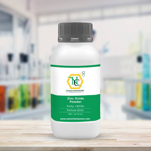
Zinc Oxide Nano-dispersion in water

Price range: $205.00 through $625.00
Select options This product has multiple variants. The options may be chosen on the product page
$625/500g
$205/100g

Product 

Zinc Oxide Nano-dispersion in water

CAS No.

1314-13-2

Appearance

Powder

Purity

≥99%,  ≥99.9%,  ≥95%

(Other purities are also available)

APS

~10–50 nm(Size Can be customized), Ask for other available size ranges.

Ingredient

N/A

Molecular Weight

81.38 g/mol

Melting Point

~1,975 °C

Boiling Point

~2,360 °C

Density

 ~5.61 g/cm³

Product Codes

NCZ-1221K

2N7 (99.7%) Vanadium (V) Pellets Evaporation Material

Price range: $205.00 through $385.00
Select options This product has multiple variants. The options may be chosen on the product page
Product 2N7 (99.7%) Vanadium (V) Pellets Evaporation Material
CAS No. 7440-62-2
Appearance Silver, Metallic 
Purity ≥99%,  ≥99.9%,  ≥95%(Other purities are also available)
APS 1–10 mm (Size Can be customized),  Ask for other available size range.
Ingredient V
Molecular Weight 50.94g/mol
Melting Point N/A
Boiling Point N/A
Density 6.11 g/cm³
Product Codes NCZ-126E
 

3N8 (99.98%) Nickel (Ni) Wire Evaporation Materials

Price range: $205.00 through $385.00
Select options This product has multiple variants. The options may be chosen on the product page
Product 3N8 (99.98%) Nickel (Ni) Wire Evaporation Materials
CAS No. 7440-02-0
Appearance Lustrous, Metallic, Silvery Tinge 
Purity ≥99%,  ≥99.9%,  ≥95%(Other purities are also available)
APS 1mm (Size Can be customized),  Ask for other available size range.
Ingredient Ni
Molecular Weight 58.69 g/mol
Melting Point 1,453 °C
Boiling Point 2,732 °C
Density 8.91 g/cm³
Product Codes NCZ-127E

1% Silver (Ag) Nanoparticle Water Dispersion, 160-180nm, >99.99% Purity

Price range: $205.00 through $385.00
Select options This product has multiple variants. The options may be chosen on the product page
Product 1% Silver (Ag) Nanoparticle Water Dispersion, 160-180nm, >99.99% Purity
CAS No. 7440-22-4
Appearance Black
Purity ≥99%,  ≥99.9%,  ≥95%(Other purities are also available)
APS 160-180nm (Size Can be customized), Ask for other available size range.
Ingredient Ag
Molecular Weight 107.87 g/mol
Melting Point N/A
Boiling Point N/A
Density N/A
Product Codes NCZ-113I
 

99.99% 4N 200 nm Alpha Aluminum Oxide (Alumina) Al2O3 Powder, 500 g

$205.00
Product 99.99% 4N 200 nm Alpha Aluminum Oxide (Alumina) Al2O3 Powder, 500 g
CAS No. 1344-28-1
Appearance White
Purity ≥99%,  ≥99.9%,  ≥95%(Other purities are also available)
APS 200nm (Size Can be customized),  Ask for other available size range.
Ingredient Al2O3
Molecular Weight 101.96 g/mol
Melting Point 2,050 °C
Boiling Point N/A
Density 3.95–4.00 g/cm³
Product Codes NCZ-240I

Aluminum Fluoride (AlF3) 99.999% Optical Grade

Price range: $205.00 through $3,175.00
Select options This product has multiple variants. The options may be chosen on the product page
Product Aluminum Fluoride (AlF3) 99.999% Optical Grade
CAS No. 7784-18-1
Appearance White, odorless solid
Purity ≥99%,  ≥99.9%,  ≥95%(Other purities are also available)
APS 20–80nm (Size Can be customized),  Ask for other available size range.
Ingredient AlF3
Molecular Weight 83.98 g/mol
Melting Point 1,290 °C
Boiling Point N/A
Density 3.10 g/cm³
Product Codes NCZ-279I

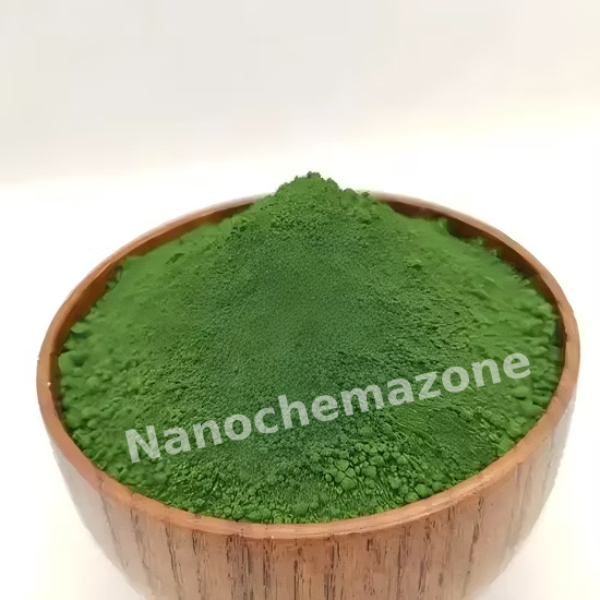
Chromium (III) Oxide (Cr2O3) 99.99% 4N Powder

Price range: $205.00 through $1,916.00
Select options This product has multiple variants. The options may be chosen on the product page
Product Chromium (III) Oxide (Cr2O3) 99.99% 4N Powder
CAS No. 1308-38-9
Appearance Green
Purity ≥99%,  ≥99.9%,  ≥95%(Other purities are also available)
APS 1–5µm (Size Can be customized),  Ask for other available size range.
Ingredient Cr2O3
Molecular Weight 151.99 g/mol
Melting Point 2,435 °C
Boiling Point N/A
Density 5.22 g/cm³
Product Codes NCZ-318I