25 ml/245 €
100 ml/586 €
500 ml/1740 €
1000 ml/2680 €
Please contact us for quotes on larger quantities !!!
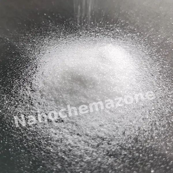
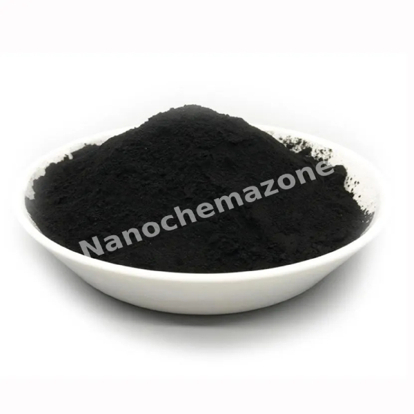
Polyhydroxylated Fullerene (Fullerenols)/ C60
(-OH) Functionalized, Dispersed in Water, 1000 ppm Dry powder
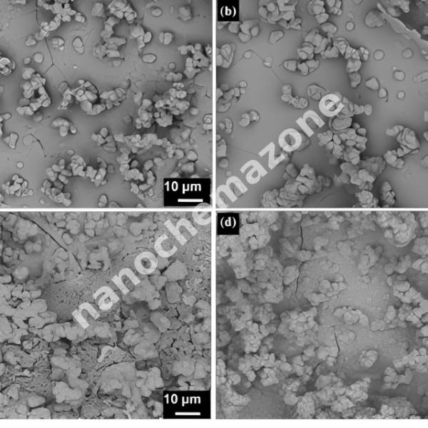
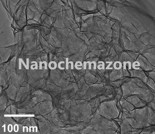
The starting material is >98% purity C60 fullerenes. C60 bearing over 40 hydroxyl groups that have higher water solubility (>50 mg/mL).
These exist as monodisperse nanoparticles in water, and have a valiant polishing effect. They exhibit superior antioxidant and anti-inflammatory properties.
Applications:
1. Pharmaceutical: Diagnostic reagents, super drugs, cosmetics, nuclear magnetic resonance (NMR) with the developer. DNA affinity, anti-HIV drugs,
anti-cancer drugs, chemotherapy drugs, cosmetics additives and scientific research.
2. Energy: Solar battery, fuel cell, secondary battery.
3. Industry: Wear resistant material, flame retardant materials, lubricants, polymer additives, high-performance membrane, catalyst, artificial diamond,
hard alloy, electric viscous fluid, ink filters, high-performance coatings, fire retardant coatings, manufacturing bioactive materials , memory materials,
embedded molecular and other characteristics, composite materials etc.
4. Information industry: Semiconductor record medium, magnetic materials, printing ink, toner, ink, paper special purposes.
5. Electronic parts: Superconducting semiconductor, diodes, transistors, inductor. ,
6. Optical materials, electronic camera, fluorescence display tube, nonlinear optical materials.
7. Environment: Gas adsorption, gas storage.