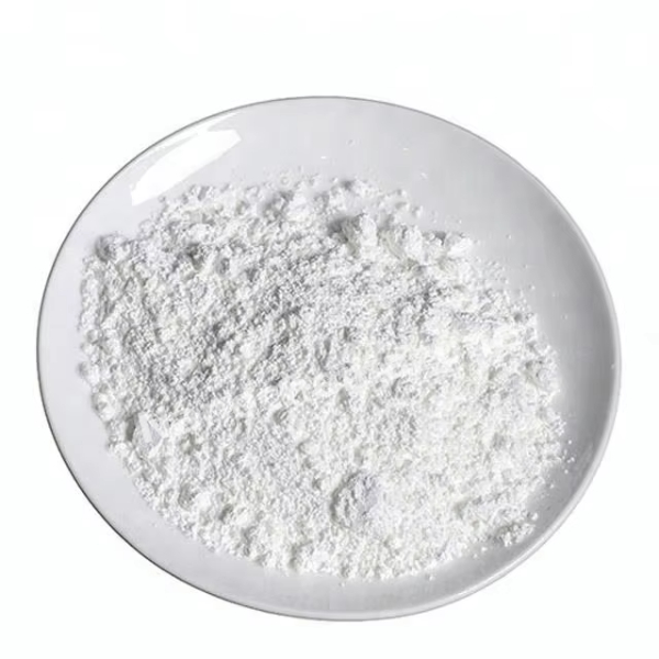
Carbon Nanotube-TiO2 Prepared by Electrostatic Adsorption, CNTs: 25 wt%, TiO2-rutile: 75 wt%

Price range: $123.00 through $564.00
Select options This product has multiple variants. The options may be chosen on the product page

Applications:

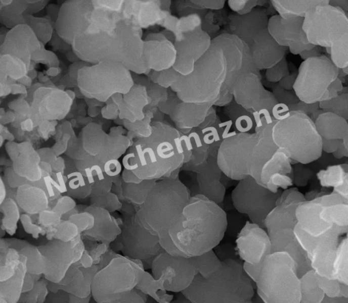
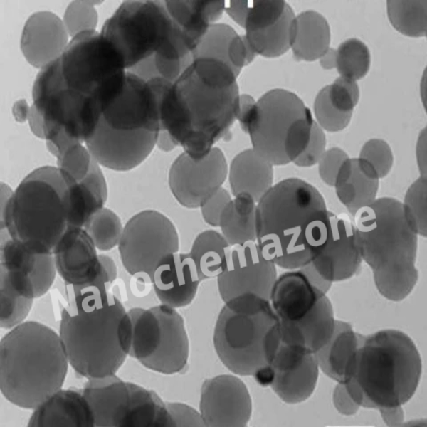
Carbon Nanotube-TiO2 is prepared by electrostatic interactions. Carbon nanotubes are treated by cationic surfactant (Cetyl trimethyl ammonium bromide). TiO2 rutile and CNTs self-assemble to form a uniform and stable complex. It is easy to disperse and has good static conductive properties. It also show excellent mechanical and corrosion resistance properties. It can be used in petrochemical industry, coal industry and many coating fields.

Graphite Sheet Thermal Interface Material, EYG Series, 1300 W/m.K, Thickness: 50 µm, Lenght: 230 mm, Width: 180 mm

Price range: $123.00 through $557.00
Select options This product has multiple variants. The options may be chosen on the product page
1 piece /123 € 5 pieces / 557 € Please contact us for quotes on larger quantities !   Graphite Sheet

Lithium Lanthanum Tantalum Zirconate (LLZTO), Size: 1-3 µm, Purity: ≥99.5

Price range: $123.00 through $1,850.00
Select options This product has multiple variants. The options may be chosen on the product page
APPLICATIONS
Lithium Lanthanum Tantalum Zirconate is used as a solid electrolyte material for Li-based batteries because of its high Lithium ionic conductivity and chemical stability with respect to lithium as well as its stability at elevated temperatures.

Aluminum (Al) Sputtering Targets, Purity: 99.999%, Size: 2”, Thickness: 0.250”

$123.00

Applications of Sputtering Targets;

  • Sputtering targets is used for film deposition. The deposition made by sputter targets is a method of depositing thin films by sputtering that involves eroding material from a "target" source onto a "substrate" such as  a silicon wafer.
  • Semiconductor sputtering targets is used to etch the target. Sputter etching is chosen in cases where a high degree of etching anisotropy is needed and selectivity is not a concern.
  • Sputter targets is also used for analysis by etching away the target material.
One of the example occurs in secondary ion spectroscopy (SIMS), where the target sample is sputtered at a constant rate. As the target is sputtered, the concentration and identity of sputtered atoms are measured using mass spectrometry. By helping of the sputtering target, the composition of the target material can be determined and even extremely low concentrations of impurities are detected. Sputtering target has also application area in space. Sputtering is one of the forms of space weathering, a process that changes the physical and chemical properties of airless bodies, such as asteroids and the Moon. Aluminum which has the chemical symbol of Al, is a silvery white, soft, ductile metal that is the third most abundant element. Aluminum is notable due to for its light weight, strength, durability and for its ability to resist corrosion. Aluminum forms an extremely thin but very strong layer of oxide film. Aluminum has also high thermal and electrical conductivity. Aluminum sputtering targets have a particularly fine-grained microstructure. This property of Aluminum sputtering targets ensures that you benefit from uniform erosion and a low susceptibility to particle formation throughout the sputtering process.

Cobalt (Co) Sputtering Targets, Purity: 99.95%, Size: 2”, Thickness: 0.125”

$123.00

Applications of Sputtering Targets;

Film deposition is accomplished using sputtering targets. A technique for sputtering thin films is called "deposition made by sputter targets," which entails eroding material from a "target" source onto a "substrate" like a silicon wafer. Etching of the target is done using semiconductor sputtering targets. When selectivity is not an issue and a high degree of etching anisotropy is required, sputter etching is the method of choice. By removing the target material through etching, sputter targets are also utilized for investigation. In secondary ion spectroscopy (SIMS), one example is when the target material is sputtered at a steady pace. Mass spectrometry is used to quantify the concentration and identity of spewed atoms as the target is sputtered.

The target material's composition may be ascertained and even very low concentrations of contaminants can be found with the aid of the sputtering target.

There is also an application area for sputtering targets in space. One type of space weathering that alters the chemical and physical characteristics of airless worlds like the Moon and asteroids is sputtering.

The chemical element cobalt has the atomic number 27 and the symbol Co. Cobalt is a silver-gray, hard, and shiny metal. Because it is one of only three room temperature ferromagnets with unaxial symmetry and hence suitability for digital recording, cobalt is employed in the production of high-strength, wear-resistant alloys as well as magnetic recording.

Copper Nanoparticles/Nanopowder in organic media (Cu, 5-7nm, oil-soluble, dispersible, lubricants additive)

Price range: $123.00 through $433.00
Select options This product has multiple variants. The options may be chosen on the product page
$123/100g
$315/500g
$433/1000g

Product 

Copper Nanoparticles/Nanopowder in organic media (Cu, 5-7nm, oil-soluble, dispersible, lubricants additive)

CAS No.

7440-50-8

Appearance

Powder

Purity

≥99%,  ≥99.9%,  ≥95%

(Other purities are also available)

APS

5-7nm (Size Can be customized), Ask for other available size ranges.

Ingredient

AlN

Molecular Weight

63.55 g/mol

Melting Point

1084.62 °C

Boiling Point

2562 °C

Density

8.96 g/cm³

Product Codes

NCZ-1031K

Aluminum Hydroxide Nanoparticles/Nanopowder ( Al(OH)3, high purity: 99.99%, 30-100 nm)

Price range: $123.00 through $380.00
Select options This product has multiple variants. The options may be chosen on the product page
$123/100g
$380/500g

Product 

Aluminum Hydroxide Nanoparticles/Nanopowder ( Al(OH)3, high purity: 99.99%, 30-100 nm)

CAS No.

21645-51-2

Appearance

Powder

Purity

≥99%,  ≥99.9%,  ≥95%

(Other purities are also available)

APS

30-100 nm (Size Can be customized), Ask for other available size ranges.

Ingredient

N/A

Molecular Weight

 78.00 g/mol

Melting Point

N/A

Boiling Point

 N/A

Density

~2.42 g/cm³

Product Codes

NCZ-1095K

Aluminum (Al) Sputtering Targets, Purity: 99.99%, Size: 2”, Thickness: 0.250”

$123.00

Product 

Aluminum (Al) Sputtering Targets, Purity: 99.99%, Size: 2'', Thickness: 0.250''

CAS No.

7429-90-5

Appearance

Powder

Purity

≥99%,  ≥99.9%,  ≥95%

(Other purities are also available)

APS

Al (Size Can be customized), Ask for other available size ranges.

Ingredient

N/A

Molecular Weight

26.98 g/mol

Melting Point

660.3 °C

Boiling Point

2467 °C

Density

 2.70 g/cm³

Product Codes

NCZ-1403K

Copper (Cu) Sputtering Targets, Purity: 99.99%, Size: 6”, Thickness: 0.125”

$123.00

Product 

Copper (Cu) Sputtering Targets, Purity: 99.99%, Size: 6'', Thickness: 0.125''

CAS No.

7440-50-8

Appearance

Powder

Purity

≥99%,  ≥99.9%,  ≥95%

(Other purities are also available)

APS

 N/A (Size Can be customized), Ask for other available size ranges.

Ingredient

N/A

Molecular Weight

63.55 g/mol

Melting Point

1,084 °C

Boiling Point

 2,562 °C

Density

8.96 g/cm³

Product Codes

NCZ-2257K

Iron (Fe) Sputtering Targets, Purity: 99.95%, Size: 2”, Thickness: 0.125”

$124.00

Applications of Sputtering Targets;

Film deposition is accomplished using sputtering targets. A technique for sputtering thin films is called "deposition made by sputter targets," which entails eroding material from a "target" source onto a "substrate" like a silicon wafer. Etching of the target is done using semiconductor sputtering targets. When selectivity is not an issue and a high degree of etching anisotropy is required, sputter etching is the method of choice. By removing the target material through etching, sputter targets are also utilized for investigation. In secondary ion spectroscopy (SIMS), one example is when the target material is sputtered at a steady pace. Mass spectrometry is used to quantify the concentration and identity of spewed atoms as the target is sputtered.

The target material's composition may be ascertained and even very low concentrations of contaminants can be found with the aid of the sputtering target.

There is also an application area for sputtering targets in space. One type of space weathering that alters the chemical and physical characteristics of airless worlds like the Moon and asteroids is sputtering.

Titanium Nanoparticles/ nanopowder ( Ti, 99.9% 40-60nm)

Price range: $124.00 through $356.00
Select options This product has multiple variants. The options may be chosen on the product page
$124/25g
$356/100g

Product 

Titanium Nanoparticles/ nanopowder ( Ti, 99.9% 40-60nm)

CAS No.

7440-32-6

Appearance

Powder

Purity

≥99%,  ≥99.9%,  ≥95%

(Other purities are also available)

APS

40-60nm (Size Can be customized), Ask for other available size ranges.

Ingredient

N/A

Molecular Weight

47.87 g/mol

Melting Point

1,668 °C

Boiling Point

3,287 °C

Density

4.51 g/cm³

Product Codes

NCZ-1077K

Titanium Nanoparticles/ nanopowder ( Ti, 99.9% 60-80 nm)

Price range: $124.00 through $315.00
Select options This product has multiple variants. The options may be chosen on the product page
$124/25g
$315/100g

Product 

Titanium Nanoparticles/ nanopowder ( Ti, 99.9% 60-80 nm)

CAS No.

7440-32-6

Appearance

Powder

Purity

≥99%,  ≥99.9%,  ≥95%

(Other purities are also available)

APS

60-80 nm (Size Can be customized), Ask for other available size ranges.

Ingredient

N/A

Molecular Weight

47.87 g/mol

Melting Point

1,668 °C

Boiling Point

3,287 °C

Density

4.51 g/cm³

Product Codes

NCZ-1078K

Zinc (Zn) Sputtering Targets, Purity: 99.99%, Size: 2”, Thickness: 0.250”

$124.00

Product 

Zinc (Zn) Sputtering Targets, Purity: 99.99%, Size: 2'', Thickness: 0.250''

CAS No.

7440‑66‑6

Appearance

Powder

Purity

≥99%,  ≥99.9%,  ≥95%

(Other purities are also available)

APS

Zn (black granules) (Size Can be customized), Ask for other available size ranges.

Ingredient

N/A

Molecular Weight

65.38 g/mol

Melting Point

419.5 °C

Boiling Point

 907 °C

Density

7.14 g/cm³

Product Codes

NCZ-1473K

Nickel (Ni) Sputtering Targets, Purity: 99.995%, Size: 1”, Thickness: 0.125”

$124.00

Product 

Nickel (Ni) Sputtering Targets, Purity: 99.995%, Size: 1'', Thickness: 0.125''

CAS No.

7440-02-0

Appearance

Powder

Purity

≥99%,  ≥99.9%,  ≥95%

(Other purities are also available)

APS

 N/A (Size Can be customized), Ask for other available size ranges.

Ingredient

N/A

Molecular Weight

~58.69 g/mol

Melting Point

~1,455 °C

Boiling Point

~2,913 °C

Density

~8.91 g/cm³

Product Codes

NCZ-1893K

Magnesium (Mg) Sputtering Targets, Purity: 99.95%, Size: 1”, Thickness: 0.250”

$124.00

Product 

Magnesium (Mg) Sputtering Targets, Purity: 99.95%, Size: 1'', Thickness: 0.250''

CAS No.

7439-95-4

Appearance

Powder

Purity

≥99%,  ≥99.9%,  ≥95%

(Other purities are also available)

APS

 N/A (Size Can be customized), Ask for other available size ranges.

Ingredient

N/A

Molecular Weight

 24.305 g/mol

Melting Point

 650 °C

Boiling Point

 1,090 °C

Density

1.738 g/cm³

Product Codes

NCZ-2005K

Copper (Cu) Sputtering Targets, Purity: 99.99%, Size: 4”, Thickness: 0.250”

$124.00

Product 

Copper (Cu) Sputtering Targets, Purity: 99.99%, Size: 4'', Thickness: 0.250''

CAS No.

7440-50-8

Appearance

Powder

Purity

≥99%,  ≥99.9%,  ≥95%

(Other purities are also available)

APS

 N/A (Size Can be customized), Ask for other available size ranges.

Ingredient

N/A

Molecular Weight

63.55 g/mol

Melting Point

1,084 °C

Boiling Point

 2,562 °C

Density

8.96 g/cm³

Product Codes

NCZ-2260K

Aluminum Silicon (AlSi) Sputtering Targets, Purity: 99.999%, Size: 1”, Thickness: 0.125”

$125.00

Applications of Sputtering Targets;

Film deposition is accomplished using sputtering targets. A technique for sputtering thin films is called "deposition made by sputter targets," which entails eroding material from a "target" source onto a "substrate" like a silicon wafer. Etching of the target is done using semiconductor sputtering targets. When selectivity is not an issue and a high degree of etching anisotropy is required, sputter etching is the method of choice. By removing the target material through etching, sputter targets are also utilized for investigation. In secondary ion spectroscopy (SIMS), one example is when the target material is sputtered at a steady pace. Mass spectrometry is used to quantify the concentration and identity of spewed atoms as the target is sputtered. With the sputtering target's assistance, the

It is possible to identify the target material and even detect incredibly tiny impurity amounts.

There is also an application area for sputtering targets in space. One type of space weathering that alters the chemical and physical characteristics of airless worlds like the Moon and asteroids is sputtering.

Niobium (Nb) Sputtering Target

Price range: $125.00 through $421.00
Select options This product has multiple variants. The options may be chosen on the product page

Product 

Niobium (Nb) Sputtering Target

CAS No.

7440-03-1

Appearance

Powder

Purity

≥99%,  ≥99.9%,  ≥95%

(Other purities are also available)

APS

 NA (Size Can be customized), Ask for other available size ranges.

Ingredient

N/A

Molecular Weight

92.906 g/mol

Melting Point

2,468 °C

Boiling Point

 4,927 °C

Density

 8.57 g/cm³

Product Codes

NCZ-1299K

Aluminum Silicon Copper Sputtering Target AlSiCu

Price range: $125.00 through $289.00
Select options This product has multiple variants. The options may be chosen on the product page
Product Aluminum Silicon Copper Sputtering Target AlSiCu
CAS No. 7429-90-5
Appearance Metallic, silvery-gray material
Purity ≥99%,  ≥99.9%,  ≥95%(Other purities are also available)
APS N/A
Ingredient AlSiCu
Molecular Weight 28.28 g/mol
Melting Point N/A
Boiling Point N/A
Density 3.1 g/cm³
Product Codes NCZ-100H
 

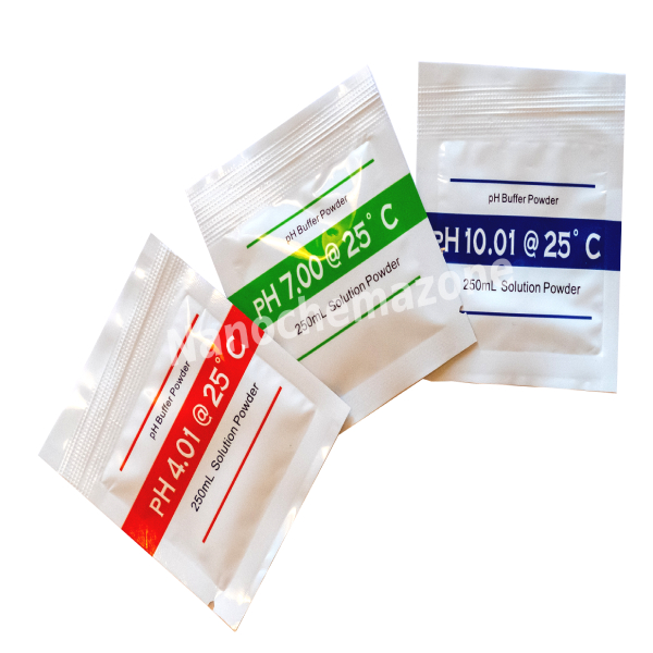
Standard pH 4.01/7.00/10.01 Buffer Powder, 3 x 10 Sachets

$125.00
Product Standard pH 4.01/7.00/10.01 Buffer Powder, 3 x 10 Sachets
CAS No. N/A
Appearance White to off-white fine crystalline
Purity ≥99%,  ≥99.9%,  ≥95%(Other purities are also available)
APS 10–100µm (Size Can be customized),  Ask for other available size range.
Ingredient KHC₈H₄O₄
Molecular Weight N/A
Melting Point N/A
Boiling Point N/A
Density 1.2–1.4 g/cm³
Product Codes NCZ-537I

Gallium Arsenide (GaAs) Wafers, Size: 2”, Thickness: 450±25 μm, Single Side Polished, EPI-ready, Dopant: Silicon (N Type)

Price range: $126.00 through $1,859.00
Select options This product has multiple variants. The options may be chosen on the product page
1 piece/114€ 5 pieces/445€ 25 pieces/1675€ Please contact us for quotes on larger quantities ! Gallium Arsenide (GaAs) Wafer Size: 2”, Single Side Polished, Thickness: 450± 25 μm, EPI-ready, Dopant: Silicon (N Type) Technical Properties:
Quality  GaAs
Materials  GaAs
Size (inch)  2”
Thickness (μm)  450± 25
Polished  Single Side
Dopant  Silicon (N Type)
Orientation  (100) =2 deg off toward<111A>± 0.5
Resistivity  ( 1.2-9.9) E-3
Mobility  1000-3000
EPD  ≤3000
Growth method  VGF
OF Length  17±1
IF Length  7±1
Applications: Gallium arsenide (GaAs) is a compound of the elements gallium and arsenic. Vertical gradient freeze is the most common method to produce GaAs wafers. Mainly used for circuits, electronics and solar cell applications. Carbon, silicon, tellurium and zinc are some of the dopants that are used to modify the characteristics and electrical properties of gallium arsenide wafers. Wafer flatness and surface purity are ensured by highest quality standards. Boron concentration of gallium arsenide wafers highly depend on the production method. Gallium arsenide wafers with adequate electrical resistancy prevent high current induction in the circuit. Mobility of GaAs wafers can be tailored with different doping levels. Gallium arsenide (GaAs) is a semiconductor compound. Gallium arsenide (GaAs)  has a high electron velocity and high saturated electron mobility. This makes gallium arsenide (GaAs) components are useful in fast electronic switching applications and at ultra-high radio frequencies. In 1907, the British discovered infrared emmission from gallium arsenide. This was called electroluminescence. Also, gallium arsenide (GaAs) was used as a solar cells in space for the Venera 3 mission in 1965, which is the first known operational use of gallium arsenide (GaAs).
  • Gallium arsenide (GaAs) is used in laser diodes.
  • Gallium arsenide (GaAs) is used in solar cells.
  • Gallium arsenide (GaAs) is used in optical windows.
  • Gallium arsenide (GaAs) is used in monolithic microwave integrated circuits.
  • Gallium arsenide (GaAs) is used in microwave frequency integrated circuits.
  • Gallium arsenide (GaAs) is used in infrared light-emitting diodes.
  • Gallium arsenide (GaAs) is useful in barometers.
  • Gallium arsenide (GaAs) is useful in pharmaceuticals and nuclear medicine tests.
  • Gallium arsenide (GaAs) is useful in high temperature thermometers.

Praseodymium (Pr) Sputtering Targets, Purity: 99.9%, Size: 2”, Thickness: 0.125”

$126.00

Applications of Sputtering Targets;

  • Sputtering targets is used for film deposition. The deposition made by sputter targets is a method of depositing thin films by sputtering that involves eroding material from a "target" source onto a "substrate" such as  a silicon wafer.
  • Semiconductor sputtering targets is used to etch the target. Sputter etching is chosen in cases where a high degree of etching anisotropy is needed and selectivity is not a concern.
  • Sputter targets is also used for analysis by etching away the target material.
One of the example occurs in secondary ion spectroscopy (SIMS), where the target sample is sputtered at a constant rate. As the target is sputtered, the concentration and identity of sputtered atoms are measured using mass spectrometry. By helping of the sputtering target, the composition of the target material can be determined and even extremely low concentrations of impurities are detected. Sputtering target has also application area in space. Sputtering is one of the forms of space weathering, a process that changes the physical and chemical properties of airless bodies, such as asteroids and the Moon.

Praseodymium (Pr) Sputtering Targets, Purity: 99.9%, Size: 2”, Thickness: 0.125”

$126.00

Applications of Sputtering Targets;

Film deposition is accomplished using sputtering targets. A technique for sputtering thin films is called "deposition made by sputter targets," which entails eroding material from a "target" source onto a "substrate" like a silicon wafer. Etching of the target is done using semiconductor sputtering targets. When selectivity is not an issue and a high degree of etching anisotropy is required, sputter etching is the method of choice. By removing the target material through etching, sputter targets are also utilized for investigation. In secondary ion spectroscopy (SIMS), one example is when the target material is sputtered at a steady pace. Mass spectrometry is used to quantify the concentration and identity of spewed atoms as the target is sputtered.

The target material's composition may be ascertained and even very low concentrations of contaminants can be found with the aid of the sputtering target.

There is also an application area for sputtering targets in space. One type of space weathering that alters the chemical and physical characteristics of airless worlds like the Moon and asteroids is sputtering.

Molybdenum Sputtering Target Mo

Price range: $126.00 through $265.00
Select options This product has multiple variants. The options may be chosen on the product page
Product Molybdenum Sputtering Target Mo
CAS No. N/A
Appearance Grey, Metallic
Purity ≥99%,  ≥99.9%,  ≥95%(Other purities are also available)
APS N/A
Ingredient Mo
Molecular Weight 95.96 g/mol
Melting Point 2,617 °C
Boiling Point N/A
Density N/A
Product Codes NCZ-129H
 

Polyhydroxylated Fullerene (Fullerenols)/ C60, (-OH) Functionalized, Dispersed in Water, 250 ppm Dry powder

Price range: $127.00 through $2,228.00
Select options This product has multiple variants. The options may be chosen on the product page
25 ml/114 € 100 ml/345 € 500 ml/1350 € 1000 ml/1990 € Please contact us for quotes on larger quantities.

Polyhydroxylated Fullerene (Fullerenols)/ C60

(-OH) Functionalized, Dispersed in Water, 250 ppm Dry powder

The starting material is >98% purity C60 fullerenes. C60 bearing over 40 hydroxyl groups that have higher water solubility (>50 mg/mL). These exist as monodisperse nanoparticles in water, and have a valiant polishing effect. They exhibit superior antioxidant and anti-inflammatory properties.

Applications:

1. Pharmaceutical: Diagnostic reagents, super drugs, cosmetics, nuclear magnetic resonance (NMR) with the developer. DNA affinity, anti-HIV drugs, anti-cancer drugs, chemotherapy drugs, cosmetics additives and scientific research. 2. Energy: Solar battery, fuel cell, secondary battery. 3. Industry: Wear resistant material, flame retardant materials, lubricants, polymer additives, high-performance membrane, catalyst, artificial diamond, hard alloy, electric viscous fluid, ink filters, high-performance coatings, fire retardant coatings, manufacturing bioactive materials , memory materials, embedded molecular and other characteristics, composite materials etc. 4. Information industry: Semiconductor record medium, magnetic materials, printing ink, toner, ink, paper special purposes. 5. Electronic parts: Superconducting semiconductor, diodes, transistors, inductor.  , 6. Optical materials, electronic camera, fluorescence display tube, nonlinear optical materials. 7. Environment: Gas adsorption, gas storage.  

Vanadium (V) Sputtering Targets, Purity: 99.5%, Size: 1”, Thickness: 0.125”

$127.00

Product 

Vanadium (V) Sputtering Targets, Purity: 99.5%, Size: 1'', Thickness: 0.125''

CAS No.

7440-62-2

Appearance

Powder

Purity

≥99%,  ≥99.9%,  ≥95%

(Other purities are also available)

APS

N/A  (Size Can be customized), Ask for other available size ranges.

Ingredient

N/A

Molecular Weight

50.9415 g/mol

Melting Point

1910 °C

Boiling Point

3407 °C

Density

6.11 g/cm³

Product Codes

NCZ-1551K

Tungsten (W) Sputtering Targets, Purity: 99.95%, Size: 1”, Thickness: 0.250”

$127.00

Product 

Tungsten (W) Sputtering Targets, Purity: 99.95%, Size: 1'', Thickness: 0.250''

CAS No.

7440-33-7

Appearance

Powder

Purity

≥99%,  ≥99.9%,  ≥95%

(Other purities are also available)

APS

N/A  (Size Can be customized), Ask for other available size ranges.

Ingredient

N/A

Molecular Weight

 183.84 g/mol

Melting Point

3422 °C

Boiling Point

 5555 °C

Density

19.25 g/cm³

Product Codes

NCZ-1594K

PAMAM dendrimer(Ethylenediamine core) -NH2 End Group

Price range: $127.00 through $2,475.00
Select options This product has multiple variants. The options may be chosen on the product page
PAMAM dendrimer(Ethylenediamine core) -NH2 End Group  
  PAMAM   Grade   GENERATION   End Group No. of End Group   Molecular Weight   Molecular Formula   Price($/g)


 -NH2

End

Group

NCZ-lOOA 0 -NH2 4 517 C22H48N1004 127
NCZ-llOA 1 -NH2 8 1430 C62H128N26012 265
NCZ-120A 2 -NH2 16 3256 C142H288N58028 379
NCZ-130A 3 -NH2 32 6909 C302H608N122060 425
NCZ-140A 4 -NH2 64 14215 C622Hl248N2500124 615
NCZ-150A 5 -NH2 128 28826 C1262H2528N5060252 765
NCZ-160A 6 -NH2 256 58048 C2542H5088N10180508 1375
NCZ-170A 7 -NH2 512 116493 C5102H10208N204201020 1755
NCZ-180A 8 -NH2 1024 233383 C10222H20448N409002044 2475
Product Codes- NCZ-2621K  

PAMAM dendrimer(Ethylenediamine core) -OH End Group

Price range: $127.00 through $765.00
Select options This product has multiple variants. The options may be chosen on the product page
PAMAM dendrimer(Ethylenediamine core) -OH  End Group  
      -OH End Group lOOH 0 -OH 4 521 C22H44N608 127
110H 1 -OH 8 1438 C62H120N18020 265
120H 2 -OH 16 3272 C142H272N42044 379
130H 3 -OH 32 6941 C302H576N90092 425
140H 4 -OH 64 14279 C622Hll84Nl860188 615
150H 5 -OH 128 30551 C1262H2400N3780480 765
  Product Codes- NCZ-2622K  

PAMAM dendrimer(Ethylenediamine core)-COOH End Group

Price range: $127.00 through $765.00
Select options This product has multiple variants. The options may be chosen on the product page
PAMAM dendrimer(Ethylenediamine core) –COOH End Group  
    -COOH End Group lOOC 0 -COOH 4 917 C38H64N10016 127
llOC 1 -COOH 8 2230 C94Hl60N26036 265
120C 2 -COOH 16 4856 C206H352N58076 379
130C 3 -COOH 32 10109 C430H736N1220156 425
140C 4 -COOH 64 20619 C878H1504N2500316 615
150C 5 -COOH 128 41635 C1774H3040N5060636 765
  Product Codes- NCZ-2623K

Aluminum (Al) Sputtering Targets, Purity: 99.999%, Size: 1”, Thickness: 0.250”

$128.00

 Applications of Sputtering Targets;

  • Sputtering targets is used for film deposition. The deposition made by sputter targets is a method of depositing thin films by sputtering that involves eroding material from a "target" source onto a "substrate" such as  a silicon wafer.
  • Semiconductor sputtering targets is used to etch the target. Sputter etching is chosen in cases where a high degree of etching anisotropy is needed and selectivity is not a concern.
  • Sputter targets is also used for analysis by etching away the target material.
One of the example occurs in secondary ion spectroscopy (SIMS), where the target sample is sputtered at a constant rate. As the target is sputtered, the concentration and identity of sputtered atoms are measured using mass spectrometry. By helping of the sputtering target, the composition of the target material can be determined and even extremely low concentrations of impurities are detected. Sputtering target has also application area in space. Sputtering is one of the forms of space weathering, a process that changes the physical and chemical properties of airless bodies, such as asteroids and the Moon. Aluminum which has the chemical symbol of Al, is a silvery white, soft, ductile metal that is the third most abundant element. Aluminum is notable due to for its light weight, strength, durability and for its ability to resist corrosion. Aluminum forms an extremely thin but very strong layer of oxide film. Aluminum has also high thermal and electrical conductivity. Aluminum sputtering targets have a particularly fine-grained microstructure. This property of Aluminum sputtering targets ensures that you benefit from uniform erosion and a low susceptibility to particle formation throughout the sputtering process.

Indium (In) Sputtering Targets, Purity: 99.99%, Size: 1”, Thickness: 0.125”

$128.00

Applications of Sputtering Targets;

Film deposition is accomplished using sputtering targets. A technique for sputtering thin films is called "deposition made by sputter targets," which entails eroding material from a "target" source onto a "substrate" like a silicon wafer. Etching of the target is done using semiconductor sputtering targets. When selectivity is not an issue and a high degree of etching anisotropy is required, sputter etching is the method of choice. By removing the target material through etching, sputter targets are also utilized for investigation. In secondary ion spectroscopy (SIMS), one example is when the target material is sputtered at a steady pace. Mass spectrometry is used to quantify the concentration and identity of spewed atoms as the target is sputtered.

The target material's composition may be ascertained and even very low concentrations of contaminants can be found with the aid of the sputtering target.

There is also an application area for sputtering targets in space. One type of space weathering that alters the chemical and physical characteristics of airless worlds like the Moon and asteroids is sputtering.

Molybdenum (Mo) Sputtering Targets, Purity: 99.95%, Size: 1”, Thickness: 0.125”

$128.00

Applications of Sputtering Targets;

Film deposition is accomplished using sputtering targets. A technique for sputtering thin films is called "deposition made by sputter targets," which entails eroding material from a "target" source onto a "substrate" like a silicon wafer. Etching of the target is done using semiconductor sputtering targets. When selectivity is not an issue and a high degree of etching anisotropy is required, sputter etching is the method of choice. By removing the target material through etching, sputter targets are also utilized for investigation. In secondary ion spectroscopy (SIMS), one example is when the target material is sputtered at a steady pace. Mass spectrometry is used to quantify the concentration and identity of spewed atoms as the target is sputtered.

By helping of the sputtering target, the composition of the target material may be evaluated and even extremely tiny amounts of contaminants are recognized.

There is also an application area for sputtering targets in space. One type of space weathering that alters the chemical and physical characteristics of airless worlds like the Moon and asteroids is sputtering.

Nickel (Ni) Sputtering Targets, Purity: 99.9%, Size: 3”, Thickness: 0.125”

$128.00

Applications of Sputtering Targets;

Film deposition is accomplished using sputtering targets. A technique for sputtering thin films is called "deposition made by sputter targets," which entails eroding material from a "target" source onto a "substrate" like a silicon wafer. Etching of the target is done using semiconductor sputtering targets. When selectivity is not an issue and a high degree of etching anisotropy is required, sputter etching is the method of choice. By removing the target material through etching, sputter targets are also utilized for investigation. In secondary ion spectroscopy (SIMS), one example is when the target material is sputtered at a steady pace. Mass spectrometry is used to quantify the concentration and identity of spewed atoms as the target is sputtered.

By helping of the sputtering target, the composition of the target material may be evaluated and even extremely tiny amounts of contaminants are recognized.

There is also an application area for sputtering targets in space. One type of space weathering that alters the chemical and physical characteristics of airless worlds like the Moon and asteroids is sputtering.

Silicon Dioxide (SiO2) Sputtering Targets, Fused Quartz, Purity: 99.995%, Size: 3”, Thickness: 0.125”

$128.00

Applications of Sputtering Targets;

Film deposition is accomplished using sputtering targets. A technique for sputtering thin films is called "deposition made by sputter targets," which entails eroding material from a "target" source onto a "substrate" like a silicon wafer. Etching of the target is done using semiconductor sputtering targets. When selectivity is not an issue and a high degree of etching anisotropy is required, sputter etching is the method of choice. By removing the target material through etching, sputter targets are also utilized for investigation. In secondary ion spectroscopy (SIMS), one example is when the target material is sputtered at a steady pace. Mass spectrometry is used to quantify the concentration and identity of spewed atoms as the target is sputtered.

The target material's composition may be ascertained and even very low concentrations of contaminants can be found with the aid of the sputtering target.

There is also an application area for sputtering targets in space. One type of space weathering that alters the chemical and physical characteristics of airless worlds like the Moon and asteroids is sputtering.

Hydroxylapatite Nanoparticles / Nanopowder (Ca10(PO4)6(OH)2)

Price range: $128.00 through $789.00
Select options This product has multiple variants. The options may be chosen on the product page
$128/100g
$413/500g
$789/kg

Product 

Hydroxylapatite Nanoparticles / Nanopowder (Ca10(PO4)6(OH)2)

CAS No.

1306-06-5

Appearance

Powder

Purity

≥99%,  ≥99.9%,  ≥95%

(Other purities are also available)

APS

<40nm (Size Can be customized), Ask for other available size ranges.

Ingredient

N/A

Molecular Weight

1004.64 g/mol

Melting Point

Decomposes >1,100 °C

Boiling Point

N/A

Density

 ~3.1 g/cm³

Product Codes

NCZ-1116K

Europium Oxide Nanoparticles / Nanopowder (Eu2O3, 99.9%, 50nm)

Price range: $128.00 through $360.00
Select options This product has multiple variants. The options may be chosen on the product page
$128/5g
$360/25g

Product 

Europium Oxide Nanoparticles / Nanopowder (Eu2O3, 99.9%, 50nm)

CAS No.

12061-16-4

Appearance

Powder

Purity

≥99%,  ≥99.9%,  ≥95%

(Other purities are also available)

APS

50nm (Size Can be customized), Ask for other available size ranges.

Ingredient

N/A

Molecular Weight

382.52 g/mol

Melting Point

~2,340 °C

Boiling Point

~3,800 °C

Density

~8.64 g/cm³

Product Codes

NCZ-1133K

Europium Oxide Nanopowder / Nanoparticles (Eu2O3, 99.9%, 50 nm)

Price range: $128.00 through $360.00
Select options This product has multiple variants. The options may be chosen on the product page
$128/5g $360/25g
Product Europium Oxide Nanopowder / Nanoparticles (Eu2O3, 99.9%, 50 nm)
CAS No. 1308-96-9
Appearance Fine white powder
Purity ≥99%,  ≥99.9%,  ≥95%(Other purities are also available)
APS 50nm (Size Can be customized),  Ask for other available size range.
Ingredient Eu2O3
Molecular Weight 351.93g/mol
Melting Point 2400°C
Boiling Point N/A
Density 7.42g/cm³
Product Codes NCZ-109R
 

300 nm High Purity 99.99% Alpha Aluminum Oxide Nanoparticles

Price range: $128.00 through $205.00
Select options This product has multiple variants. The options may be chosen on the product page
Product 300 nm High Purity 99.99% Alpha Aluminum Oxide Nanoparticles
CAS No. 1344-28-1
Appearance White
Purity ≥99%,  ≥99.9%,  ≥95%(Other purities are also available)
APS 300nm (Size Can be customized),  Ask for other available size range.
Ingredient Al₂O₃
Molecular Weight N/A
Melting Point N/A
Boiling Point N/A
Density N/A
Product Codes NCZ-153I
 

500 nm High Purity 99.99% Alpha Aluminum Oxide Nanoparticles

Price range: $128.00 through $205.00
Select options This product has multiple variants. The options may be chosen on the product page
Product 500 nm High Purity 99.99% Alpha Aluminum Oxide Nanoparticles
CAS No. 1344-28-1
Appearance White
Purity ≥99%,  ≥99.9%,  ≥95%(Other purities are also available)
APS 500nm (Size Can be customized),  Ask for other available size range.
Ingredient Al2O3
Molecular Weight N/A
Melting Point N/A
Boiling Point N/A
Density 101.96 g/cm³
Product Codes NCZ-186I
 

Niobium (Nb) Sputtering Targets, Purity: 99.95% pure Ex Ta, Size: 1”, Thickness: 0.250”

$128.00

Product 

Niobium (Nb) Sputtering Targets, Purity: 99.95% pure Ex Ta, Size: 1'', Thickness: 0.250''

CAS No.

7440-03-1

Appearance

Powder

Purity

≥99%,  ≥99.9%,  ≥95%

(Other purities are also available)

APS

N/A (Size Can be customized), Ask for other available size ranges.

Ingredient

N/A

Molecular Weight

92.906 g/mol

Melting Point

 2,468 °C

Boiling Point

 4,744 °C

Density

 8.57 g/cm³

Product Codes

NCZ-1819K

Niobium (V) Pentoxide (Nb2O5) 99.99% 4N Powder

Price range: $128.00 through $865.00
Select options This product has multiple variants. The options may be chosen on the product page
Product Niobium (V) Pentoxide (Nb2O5) 99.99% 4N Powder
CAS No. 1313-96-8
Appearance Off-white to very light yellow
Purity ≥99%,  ≥99.9%,  ≥95%(Other purities are also available)
APS 100nm (Size Can be customized),  Ask for other available size range.
Ingredient Nb2O5
Molecular Weight 265.81 g/mol
Melting Point N/A
Boiling Point N/A
Density 4.47–4.60 g/cm³
Product Codes NCZ-478I
 

Thulium (Tm) Micron Powder Purity: 99.5 %, Size: 325 mesh

Price range: $129.00 through $8,207.00
Select options This product has multiple variants. The options may be chosen on the product page
1 gram/115 € 5 grams/480 € 25 grams/1985 € 100 grams/7280 € 

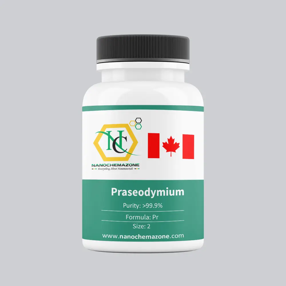
Carbon Nanotube-TiO2 Prepared by Electrostatic Adsorption, CNTs: 25 wt%, TiO2-rutile: 75 wt%

Price range: $129.00 through $609.00
Select options This product has multiple variants. The options may be chosen on the product page
Carbon Nanotube-TiO2 Prepared by Electrostatic Adsorption CNTs: 25 wt%, TiO2-rutile: 75 wt% Technical Properties: Carbon Nanotubes Purity > 95 wt%

Zinc (Zn) Sputtering Targets, Purity: 99.95%, Size: 2”, Thickness: 0.125”

$129.00

Applications of Sputtering Targets;

Film deposition is accomplished using sputtering targets. A technique for sputtering thin films is called "deposition made by sputter targets," which entails eroding material from a "target" source onto a "substrate" like a silicon wafer. Etching of the target is done using semiconductor sputtering targets. When selectivity is not an issue and a high degree of etching anisotropy is required, sputter etching is the method of choice. By removing the target material through etching, sputter targets are also utilized for investigation. In secondary ion spectroscopy (SIMS), one example is when the target material is sputtered at a steady pace. Mass spectrometry is used to quantify the concentration and identity of spewed atoms as the target is sputtered.

The target material's composition may be ascertained and even very low concentrations of contaminants can be found with the aid of the sputtering target.

There is also an application area for sputtering targets in space. One type of space weathering that alters the chemical and physical characteristics of airless worlds like the Moon and asteroids is sputtering.

Aluminum Silicon (AlSi) Sputtering Targets, Purity: 99.999%, Size: 2”, Thickness: 0.125”

$130.00

Applications of Sputtering Targets;

Film deposition is accomplished using sputtering targets. A technique for sputtering thin films is called "deposition made by sputter targets," which entails eroding material from a "target" source onto a "substrate" like a silicon wafer. Etching of the target is done using semiconductor sputtering targets. When selectivity is not an issue and a high degree of etching anisotropy is required, sputter etching is the method of choice. By removing the target material through etching, sputter targets are also utilized for investigation. In secondary ion spectroscopy (SIMS), one example is when the target material is sputtered at a steady pace. When the target shatters,

Mass spectrometry measures the concentration and identity of sputtered atoms. The target material's composition may be ascertained and even very low concentrations of contaminants can be found with the aid of the sputtering target.

There is also an application area for sputtering targets in space. One type of space weathering that alters the chemical and physical characteristics of airless worlds like the Moon and asteroids is sputtering.

Iron (Fe) Sputtering Targets, Purity: 99.99%, Size: 2”, Thickness: 0.125”

$130.00

Applications of Sputtering Targets;

Film deposition is accomplished using sputtering targets. A technique for sputtering thin films is called "deposition made by sputter targets," which entails eroding material from a "target" source onto a "substrate" like a silicon wafer. Etching of the target is done using semiconductor sputtering targets. When selectivity is not an issue and a high degree of etching anisotropy is required, sputter etching is the method of choice. By removing the target material through etching, sputter targets are also utilized for investigation. In secondary ion spectroscopy (SIMS), one example is when the target material is sputtered at a steady pace. Mass spectrometry is used to quantify the concentration and identity of spewed atoms as the target is sputtered.

The target material's composition may be ascertained and even very low concentrations of contaminants can be found with the aid of the sputtering target.

There is also an application area for sputtering targets in space. One type of space weathering that alters the chemical and physical characteristics of airless worlds like the Moon and asteroids is sputtering.

Aluminum Oxide Powder (Alumina, alpha-Al2O3, 99.999%, 0.5-10 um)

Price range: $130.00 through $391.00
Select options This product has multiple variants. The options may be chosen on the product page
$135/100g
$282/500g $396/1kg

Product

Aluminum Oxide Powder (Alumina, alpha-Al2O3, 99.999%, 0.5-10 um)
CAS No. 1344-28-1

Appearance

Powder

Purity

≥99%,  ≥99.9%,  ≥95%

(Other purities are also available)

APS

0.5–10 µm (Size Can be customized), Ask for other available size ranges.

Ingredient

N/A

Molecular Weight

101.96 g/mol

Melting Point

2,072°C

Boiling Point

2980 °C (5400 °F)

Density

3.60g/cm

Product Codes

NCZ-1087K

Zinc Sputtering Target Zn

Price range: $130.00 through $321.00
Select options This product has multiple variants. The options may be chosen on the product page
Product Zinc Sputtering Target Zn
CAS No. 7440-66-6
Appearance Shiny silvery-grey metal
Purity ≥99%,  ≥99.9%,  ≥95%(Other purities are also available)
APS N/A
Ingredient Zn
Molecular Weight 65.38 g/mol.
Melting Point N/A
Boiling Point N/A
Density 7.14 g/cm³
Product Codes NCZ-149H
 

5N (99.999%) Bismuth (Bi) Pieces Evaporation Materials

Price range: $131.00 through $1,189.00
Select options This product has multiple variants. The options may be chosen on the product page
Product 5N (99.999%) Bismuth (Bi) Pieces Evaporation Materials
CAS No. 7440-69-9
Appearance Lustrous Reddish White, Metallic 
Purity ≥99%,  ≥99.9%,  ≥95%(Other purities are also available)
APS 3–6mm (Size Can be customized),  Ask for other available size range.
Ingredient Bi
Molecular Weight 144.24 g/mol
Melting Point 271°C
Boiling Point 1564°C
Density 9.8 g/cm³
Product Codes NCZ-112E

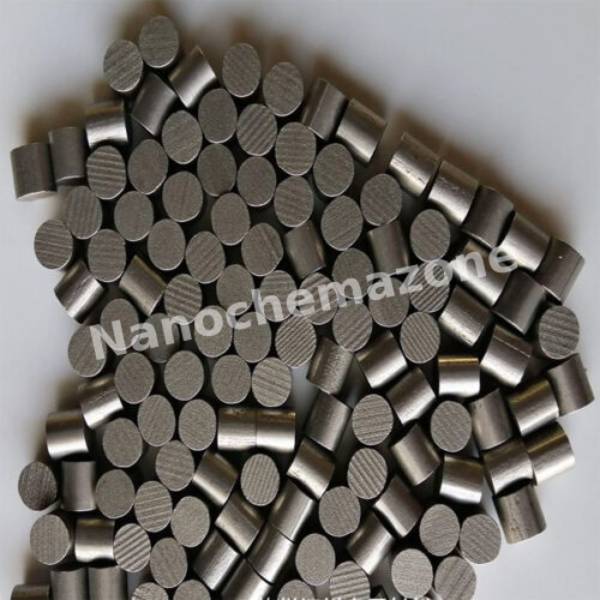
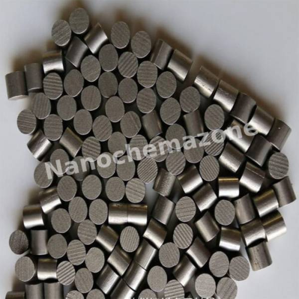
Vanadium (V) Sputtering Targets, Purity: 99.5%, Size: 1”, Thickness: 0.250”

$131.00

Product 

Vanadium (V) Sputtering Targets, Purity: 99.5%, Size: 1'', Thickness: 0.250''

CAS No.

7440-62-2

Appearance

Powder

Purity

≥99%,  ≥99.9%,  ≥95%

(Other purities are also available)

APS

N/A  (Size Can be customized), Ask for other available size ranges.

Ingredient

N/A

Molecular Weight

50.9415 g/mol

Melting Point

1910 °C

Boiling Point

3407 °C

Density

6.11 g/cm³

Product Codes

NCZ-1550K

5N (99.999%) Bismuth (Bi) Pieces Evaporation Materials

Price range: $131.00 through $1,189.00
Select options This product has multiple variants. The options may be chosen on the product page
Product 5N (99.999%) Bismuth (Bi) Pieces Evaporation Materials
CAS No. 7440-69-9
Appearance Silvery-white to pinkish metallic solid
Purity ≥99%,  ≥99.9%,  ≥95%(Other purities are also available)
APS N/A
Ingredient Bi
Molecular Weight 08.98 g/mol
Melting Point 271.4 °C
Boiling Point 1,564 °C
Density 9.78 g/cm³
Product Codes NCZ-195I

Tin (Sn) Sputtering Targets, Purity: 99.95%, Size: 2”, Thickness: 0.125”

$131.00

Product 

Tin (Sn) Sputtering Targets, Purity: 99.95%, Size: 2'', Thickness: 0.125''

CAS No.

7440-31-5

Appearance

Powder

Purity

≥99%,  ≥99.9%,  ≥95%

(Other purities are also available)

APS

N/A  (Size Can be customized), Ask for other available size ranges.

Ingredient

N/A

Molecular Weight

118.71 g/mol

Melting Point

231.93 °C

Boiling Point

2602 °C

Density

~7.31 g/cm³

Product Codes

NCZ-1643K

Selenium (Se) Sputtering Targets, Purity: 99.999%, Size: 1”, Thickness: 0.250”

$131.00

Product 

Selenium (Se) Sputtering Targets, Purity: 99.999%, Size: 1'', Thickness: 0.250''

CAS No.

7782-49-2

Appearance

Powder

Purity

≥99%,  ≥99.9%,  ≥95%

(Other purities are also available)

APS

N/A  (Size Can be customized), Ask for other available size ranges.

Ingredient

N/A

Molecular Weight

 78.96 g/mol

Melting Point

 221 °C

Boiling Point

 685 °C

Density

 4.81 g/cm³

Product Codes

NCZ-1773K

Selenium (Se) Sputtering Targets, Purity: 99.999%, Size:1”, Thickness: 0.125”

$131.00

Product 

Selenium (Se) Sputtering Targets, Purity: 99.999%, Size:1'', Thickness: 0.125''

CAS No.

7782-49-2

Appearance

Powder

Purity

≥99%,  ≥99.9%,  ≥95%

(Other purities are also available)

APS

N/A  (Size Can be customized), Ask for other available size ranges.

Ingredient

N/A

Molecular Weight

 78.96 g/mol

Melting Point

 221 °C

Boiling Point

 685 °C

Density

 4.81 g/cm³

Product Codes

NCZ-1774K

Cobalt (Co) Sputtering Targets, Purity: 99.95%, Size: 2”, Thickness: 0.250”

$131.00

Product 

Cobalt (Co) Sputtering Targets, Purity: 99.95%, Size: 2'', Thickness: 0.250''

CAS No.

7440‑48‑4

Appearance

Powder

Purity

≥99%,  ≥99.9%,  ≥95%

(Other purities are also available)

APS

 N/A (Size Can be customized), Ask for other available size ranges.

Ingredient

N/A

Molecular Weight

58.93 g/mol (cobalt atomic weight)

Melting Point

~1,495 °C

Boiling Point

~2,870–2,927 °C

Density

~8.9 g/cm³

Product Codes

NCZ-2292K

Copper (Cu) Nanopowder/Nanoparticles, Purity: 99.95%, Size: 65 nm, Metal Basis

Price range: $132.00 through $1,457.00
Select options This product has multiple variants. The options may be chosen on the product page

Copper (Cu) Nanopowder/Nanoparticles

Purity: 99.95%, Size: 65 nm, Metal Basis

Technical Properties:

Bulk Density (g/cm3) 0,22
True Density (g/cm3) 8,9
Color warm copper brown
Shape spherical
Crystal Structure cubic
Average Particle Size (nm) 65
Specific Surface Area (m2/g) 6,5-7,5
Elemental Analysis Cu Fe Ni Others
99.9 0.006 0.005 0.002

Properties, Storage and Cautions:

Copper nanoparticles are highly reactive and flammable, therefore it should be handled with care and rapid moves, vibrations should be avoided. Nanopowder should be kept away from sunlight, any kind of heating, moisture and impacts. Coagulation of the particles is a serious problem, so, nanopowder should be sealed under vacuum and should be kept in cool and dry conditions. Air contact should be avoided.

Magnesium (Mg) Sputtering Targets, Purity: 99.98%, Size: 1”, Thickness: 0.125”

$132.00

Applications of Sputtering Targets;

Film deposition is accomplished using sputtering targets. A technique for sputtering thin films is called "deposition made by sputter targets," which entails eroding material from a "target" source onto a "substrate" like a silicon wafer. Etching of the target is done using semiconductor sputtering targets. When selectivity is not an issue and a high degree of etching anisotropy is required, sputter etching is the method of choice. By removing the target material through etching, sputter targets are also utilized for investigation. In secondary ion spectroscopy (SIMS), one example is when the target material is sputtered at a steady pace. Mass spectrometry is used to quantify the concentration and identity of spewed atoms as the target is sputtered.

By helping of the sputtering target, the composition of the target material may be evaluated and even extremely tiny amounts of contaminants are recognized.

There is also an application area for sputtering targets in space. One type of space weathering that alters the chemical and physical characteristics of airless worlds like the Moon and asteroids is sputtering.

3N (99.9%) Silicon Nitride (Si3N4) Pieces Evaporation Materials

$132.00
Select options This product has multiple variants. The options may be chosen on the product page
Product 3N (99.9%) Silicon Nitride (Si3N4) Pieces Evaporation Materials
CAS No. 1308-38-9
Appearance White to Grey/Solid
Purity ≥99%,  ≥99.9%,  ≥95%(Other purities are also available)
APS 3-6mm (Size Can be customized),  Ask for other available size range.
Ingredient Cr2O3
Molecular Weight 151.99 g/mol
Melting Point 1,900 °C
Boiling Point N/A
Density 3.17 g/cm3
Product Codes NCZ-164E

Zinc (Zn) Sputtering Targets, Purity: 99.95%, Size: 1”, Thickness: 0.250”

$132.00

Product 

Zinc (Zn) Sputtering Targets, Purity: 99.95%, Size: 1'', Thickness: 0.250''

CAS No.

7440‑66‑6

Appearance

Powder

Purity

≥99%,  ≥99.9%,  ≥95%

(Other purities are also available)

APS

Zn (black granules) (Size Can be customized), Ask for other available size ranges.

Ingredient

N/A

Molecular Weight

65.38 g/mol

Melting Point

419.5 °C

Boiling Point

 907 °C

Density

7.14 g/cm³

Product Codes

NCZ-1476K