High Temperature Teflon Tape for Lithium Battery, Width: 19 mm, Thickness: 0.13 mm, Length: 10 m

Price range: $75.00 through $235.00
Select options This product has multiple variants. The options may be chosen on the product page

Applications:

High Temperature Teflon Tape for Lithium Battery is mainly used to prevent the battery from being high temperature scald.

Conductive Acetylene Black for Li-ion Battery Anode/Cathode

Price range: $75.00 through $138.00
Select options This product has multiple variants. The options may be chosen on the product page

Applications:

Conductive Acetylene Black for Li-ion Battery Anode/Cathode is used for preparing Li-ion battery electrode material and conducting material, for example: Cathode: Cathode Active+Acetylene Black (Conductive)+PVDF+NMP Anode: Anode Active+Acetylene Black (Conductive)+PVDF+NMP (or SBR+CMC)  

(-COOH) Functionalized Industrial Short Multi Walled Carbon Nanotubes, Purity: > 92%, Outside Diameter: 28-48 nm

Price range: $75.00 through $460.00
Select options This product has multiple variants. The options may be chosen on the product page

Applications:

Multi Walled Carbon Nanotubes have a wide range of possible uses in several industries. These applications span a variety of fields, including energy, chemistry, mechanics, and electric-electronics. It can be used for a number of things, including medication administration, biosensors, CNT composites, catalysis, nanoprobes, and hydrogen storage. 7, lithium-ion batteries, eight gas discharge tubes nine flat-panel screens, ten supercapacitors, and eleven transistors a dozen solar cells, 14 templates, 13 photoluminescence

Nickel-Coated Multi Walled Carbon Nanotubes, Purity: > 96%, Outside Diameter: 8-18 nm

Price range: $75.00 through $469.00
Select options This product has multiple variants. The options may be chosen on the product page

Applications:

MWCNTs are given a nickel coating to create a one-dimensional magnetic material. Ferromagnetic materials include nickel. A template for ferromagnetic nickel is made using MWCNTs. MWCNTs with nickel coating exhibit strong magnetic characteristics. MWCNTs with nickel coatings have numerous potential uses in various industries. Medicine, mechanics, electric-electronics, chemistry, energy, and other fields are among these uses. It can be used in drug delivery, biosensors, CNT composites, and other applications. four, nanoprobes, five, six, and hydrogen storage seven lithium batteries, tubes for 8 gas discharges, the nine flat panel displays, Supercapacitors ten, transistors eleven twelve solar cellstemplates, 13-photoluminescence, and 14

Graphene Oxide, 2-5 Layer, Dia: 4,5 µm, SA: 420 m2/gr

Price range: $75.00 through $742.00
Select options This product has multiple variants. The options may be chosen on the product page

Applications of Graphene Oxide

  • Composite
  • Thermal management and heat spreading
  • Graphene-polymer composite materials
  • Graphene Oxide paper
  • Transparent and conductive graphene oxide coatings
  • Solar cells
  • Supercapacitors graphene oxide
  • Low permeability materials
  • High-Barrier packaging
  • Electro-static Dissipation Graphene Oxide (ESD) films
  • Support for metallic catalysts
  • Chemical-bio  graphene oxide sensors
  • Multifunctional materials based on Graphene
  • Graphene Research

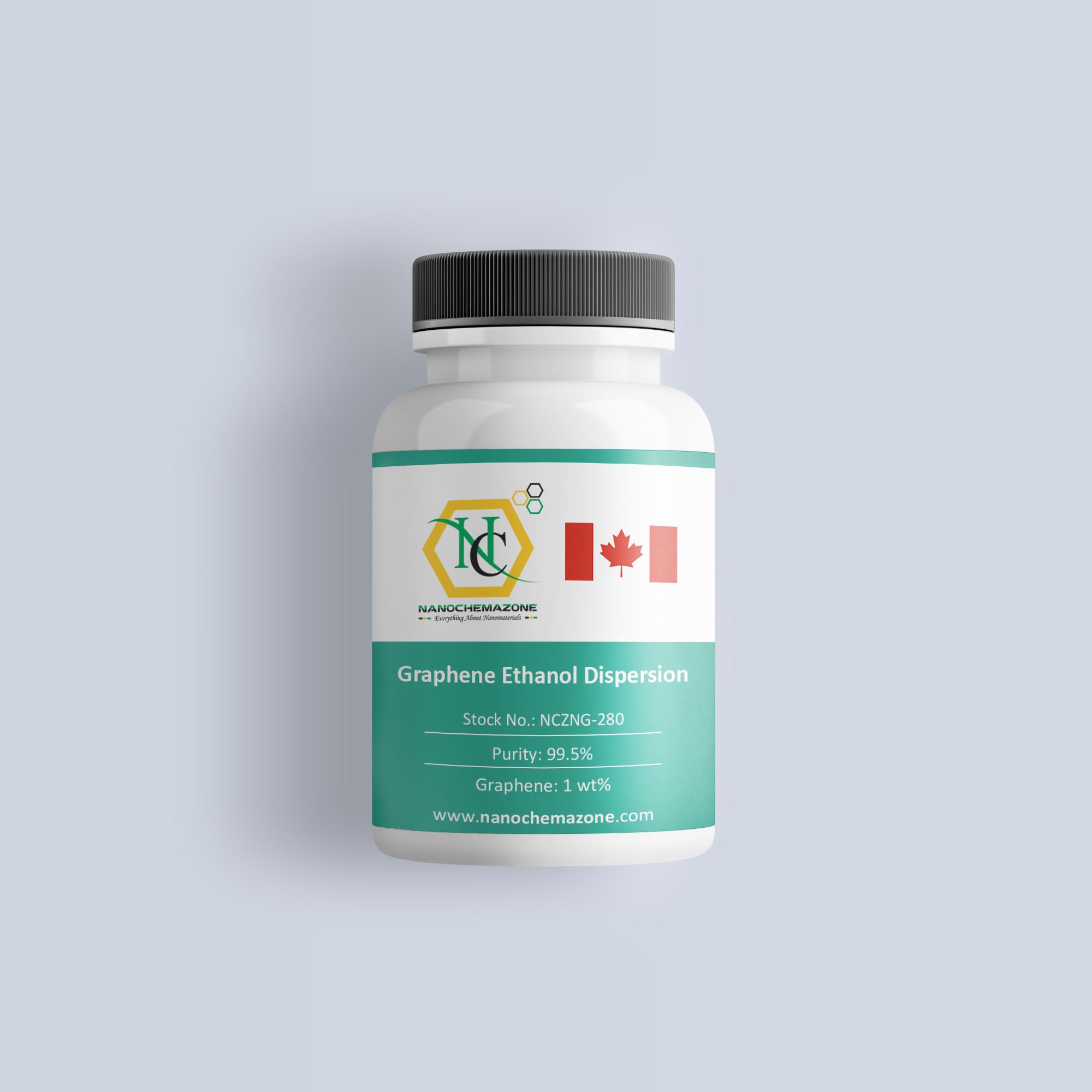
Graphene Ethanol Dispersion, Purity: 99.5%, Graphene: 1 wt%

Price range: $75.00 through $1,083.00
Select options This product has multiple variants. The options may be chosen on the product page
30 ml: 75 € 60 ml: 130 €                         

Prime Si+Si3N4 Wafer, Size: 3”, Orientation: (100), Boron Doped, Resistivity: 1-10 (ohm.cm), 2 Side Polished, Thickness: 381± 25 μm, Coating 300 nm

Price range: $75.00 through $1,620.00
Select options This product has multiple variants. The options may be chosen on the product page
Prime Si+Si3N4 Wafer Size: 3”, Orientation: (100), Boron Doped, Thickness: 381± 25 μm, Coating 300 nm Technical Properties: Quality Prime

Prime Si+SiO2 Wafer (wet), Size: 4”, Orientation: (100), Boron Doped, Resistivity: 1 – 10 (ohm.cm), 1-Side Polished, Thickness: 525 ± 25 μm, Coating 400 nm

Price range: $75.00 through $1,068.00
Select options This product has multiple variants. The options may be chosen on the product page
Prime Si+SiO2 Wafer (wet) Size: 4”, Orientation: (100), Boron Doped, 1-Side Polished, Thickness: 525 ± 25 μm, Coating 400 nm

Prime Si+SiO2 Wafer (dry), Size: 4”, Orientation: (100), Boron Doped, Resistivity: 1 -10 (ohm.cm), 1-Side Polished, Thickness: 525 ± 25 μm, Coating 200 nm

Price range: $75.00 through $1,068.00
Select options This product has multiple variants. The options may be chosen on the product page
Prime Si+SiO2 Wafer (dry) Size: 4”, Orientation: (100), Boron Doped, 1-Side Polished, Thickness: 525 ± 25 μm, Coating 200 nm

Conductive Acetylene Black for Li-ion Battery Anode/Cathode

Price range: $75.00 through $138.00
Select options This product has multiple variants. The options may be chosen on the product page

Applications:

Conductive Acetylene Black for Li-ion Battery Anode/Cathode is used for preparing Li-ion battery electrode material and conducting material, for example: Cathode: Cathode Active+Acetylene Black (Conductive)+PVDF+NMP Anode: Anode Active+Acetylene Black (Conductive)+PVDF+NMP (or SBR+CMC)

Terbium Oxide (Tb4O7) Nanopowder/Nanoparticles, Purity: 99.97%, Size: 8-110 nm, Cubic

Price range: $75.00 through $387.00
Select options This product has multiple variants. The options may be chosen on the product page

Applications:

Terbium oxide nanoparticles have good magnetic and optical properties. It is used in magneto-optical glasses, and magneto-optical recording materials. It is also used in glass materials with Faraday Rotation effect for optical and laser based devices. It has catalytic application in automobile exhaust converter, and is used as activating agent for fluorescent powder.

Praseodymium (Pr) Sputtering Targets, Purity: 99.9%, Size: 1”, Thickness: 0.250”

$75.00

Applications of Sputtering Targets;

  • Sputtering targets is used for film deposition. The deposition made by sputter targets is a method of depositing thin films by sputtering that involves eroding material from a "target" source onto a "substrate" such as  a silicon wafer.
  • Semiconductor sputtering targets is used to etch the target. Sputter etching is chosen in cases where a high degree of etching anisotropy is needed and selectivity is not a concern.
  • Sputter targets is also used for analysis by etching away the target material.
One of the example occurs in secondary ion spectroscopy (SIMS), where the target sample is sputtered at a constant rate. As the target is sputtered, the concentration and identity of sputtered atoms are measured using mass spectrometry. By helping of the sputtering target, the composition of the target material can be determined and even extremely low concentrations of impurities are detected. Sputtering target has also application area in space. Sputtering is one of the forms of space weathering, a process that changes the physical and chemical properties of airless bodies, such as asteroids and the Moon.

Praseodymium (Pr) Sputtering Targets, Purity: 99.9%, Size: 1”, Thickness: 0.125”

$75.00

Applications of Sputtering Targets;

  • Sputtering targets is used for film deposition. The deposition made by sputter targets is a method of depositing thin films by sputtering that involves eroding material from a "target" source onto a "substrate" such as  a silicon wafer.
  • Semiconductor sputtering targets is used to etch the target. Sputter etching is chosen in cases where a high degree of etching anisotropy is needed and selectivity is not a concern.
  • Sputter targets is also used for analysis by etching away the target material.
One of the example occurs in secondary ion spectroscopy (SIMS), where the target sample is sputtered at a constant rate. As the target is sputtered, the concentration and identity of sputtered atoms are measured using mass spectrometry. By helping of the sputtering target, the composition of the target material can be determined and even extremely low concentrations of impurities are detected. Sputtering target has also application area in space. Sputtering is one of the forms of space weathering, a process that changes the physical and chemical properties of airless bodies, such as asteroids and the Moon.

Graphene Oxide, 2-5 Layer, Dia: 4,5 µm, SA: 420 m2/gr

Price range: $75.00 through $742.50
Select options This product has multiple variants. The options may be chosen on the product page
1 gram / 75 € 5 grams / 269.50 € 25 grams / 742.50 €                       

Praseodymium (Pr) Sputtering Targets, Purity: 99.9%, Size: 1”, Thickness: 0.250”

$75.00

Applications of Sputtering Targets;

Film deposition is accomplished using sputtering targets. A technique for sputtering thin films is called "deposition made by sputter targets," which entails eroding material from a "target" source onto a "substrate" like a silicon wafer. Etching of the target is done using semiconductor sputtering targets. When selectivity is not an issue and a high degree of etching anisotropy is required, sputter etching is the method of choice. By removing the target material through etching, sputter targets are also utilized for investigation. In secondary ion spectroscopy (SIMS), one example is when the target material is sputtered at a steady pace. Mass spectrometry is used to quantify the concentration and identity of spewed atoms as the target is sputtered.

The target material's composition may be ascertained and even very low concentrations of contaminants can be found with the aid of the sputtering target.

There is also an application area for sputtering targets in space. One type of space weathering that alters the chemical and physical characteristics of airless worlds like the Moon and asteroids is sputtering.

Praseodymium (Pr) Sputtering Targets, Purity: 99.9%, Size: 1”, Thickness: 0.125”

$75.00

Applications of Sputtering Targets;

Film deposition is accomplished using sputtering targets. A technique for sputtering thin films is called "deposition made by sputter targets," which entails eroding material from a "target" source onto a "substrate" like a silicon wafer. Etching of the target is done using semiconductor sputtering targets. When selectivity is not an issue and a high degree of etching anisotropy is required, sputter etching is the method of choice. By removing the target material through etching, sputter targets are also utilized for investigation. In secondary ion spectroscopy (SIMS), one example is when the target material is sputtered at a steady pace. Mass spectrometry is used to quantify the concentration and identity of spewed atoms as the target is sputtered.

The target material's composition may be ascertained and even very low concentrations of contaminants can be found with the aid of the sputtering target.

There is also an application area for sputtering targets in space. One type of space weathering that alters the chemical and physical characteristics of airless worlds like the Moon and asteroids is sputtering.

Silver Nanoparticles/Nanopowder Oleic Acid Coated (Ag, 30~50nm)

Price range: $75.00 through $377.00
Select options This product has multiple variants. The options may be chosen on the product page
$75/5g $170/25g
$380/100g
 

Product 

Silver Nanoparticles/Nanopowder Oleic Acid Coated (Ag, 30~50nm)

CAS No.

24304-00-5

Appearance

Powder

Purity

≥99%,  ≥99.9%,  ≥95%

(Other purities are also available)

APS

30-50 nm (Size Can be customized), Ask for other available size ranges.

Ingredient

AlN

Molecular Weight

40.982 g/mol

Melting Point

2200 °C

Boiling Point

2517 °C

Density

3.3 g/cm³

Product Codes

NCZ-1005K

Aluminum Powder (Al) 97+%, 1-2 microns

Price range: $75.00 through $255.00
Select options This product has multiple variants. The options may be chosen on the product page
$75/100g
$170/500g
$255/1kg

Product 

Aluminum Powder (Al) 97+%, 1-2 microns

CAS No.

24304-00-5

Appearance

Powder

Purity

≥99%,  ≥99.9%,  ≥95%

(Other purities are also available)

APS

1-2 micron (Size Can be customized), Ask for other available size ranges.

Ingredient

AlN

Molecular Weight

40.982 g/mol

Melting Point

2200 °C

Boiling Point

2517 °C

Density

3.3 g/cm³

Product Codes

NCZ-1013K

Silicon Nanoparticles/ Nanopowder (Si, 99% 100 nm)

Price range: $75.00 through $282.00
Select options This product has multiple variants. The options may be chosen on the product page
$75/25g
$282/100g

Product 

Silicon Nanoparticles/ Nanopowder (Si, 99% 100 nm)

CAS No.

7440-21-3

Appearance

Powder

Purity

≥99%,  ≥99.9%,  ≥95%

(Other purities are also available)

APS

100 nm (Size Can be customized), Ask for other available size ranges.

Ingredient

N/A

Molecular Weight

28.0855 g/mol

Melting Point

 1,414 °C

Boiling Point

3,265 °C

Density

~2.33 g/cm³

Product Codes

NCZ-1065K

Zinc Powder ( Zn, 99.9%, -325 mesh)

Price range: $75.00 through $290.00
Select options This product has multiple variants. The options may be chosen on the product page
$75/100g
$175/500g
$290/kg

Product 

Zinc Powder ( Zn, 99.9%, -325 mesh)

CAS No.

7440-66-6

Appearance

Powder

Purity

≥99%,  ≥99.9%,  ≥95%

(Other purities are also available)

APS

-325 mesh (Size Can be customized), Ask for other available size ranges.

Ingredient

N/A

Molecular Weight

65.38 g/mol

Melting Point

419.5 °C

Boiling Point

907 °C

Density

7.14 g/cm³

Product Codes

NCZ-1085K

Lanthanum Oxide Nanoparticles/Nanopowder ( La2O3, 99.99%, 100nm)

Price range: $75.00 through $173.00
Select options This product has multiple variants. The options may be chosen on the product page
$75/25g
$173/100g

Product 

Lanthanum Oxide Nanoparticles/Nanopowder ( La2O3, 99.99%, 100nm)

CAS No.

1312-81-8

Appearance

Powder

Purity

≥99%,  ≥99.9%,  ≥95%

(Other purities are also available)

APS

100nm (Size Can be customized), Ask for other available size ranges.

Ingredient

N/A

Molecular Weight

 325.81 g/mol

Melting Point

~2,313 °C

Boiling Point

~4,200 °C

Density

 ~6.51 g/cm³

Product Codes

NCZ-1147K

Samarium Oxide Micronpowder( Sm2O3, 99.9%, 3~5um)

Price range: $75.00 through $181.00
Select options This product has multiple variants. The options may be chosen on the product page
$75/25g
$115/100g
$181/500g

Product 

Samarium Oxide Micronpowder( Sm2O3, 99.9%, 3~5um)

CAS No.

12060-58-1

Appearance

Powder

Purity

≥99%,  ≥99.9%,  ≥95%

(Other purities are also available)

APS

3~5um (Size Can be customized), Ask for other available size ranges.

Ingredient

N/A

Molecular Weight

348.72 g/mol

Melting Point

~2,336 °C

Boiling Point

~4,000 °C

Density

8.35 g/cm³

Product Codes

NCZ-1178K

Lanthanum Oxide Nanoparticles/ Nanopowder ( La2O3, 99.99+%, 100 nm)

Price range: $75.00 through $173.00
Select options This product has multiple variants. The options may be chosen on the product page
$75/25g $173/100g
Product Lanthanum Oxide Nanoparticles/ Nanopowder ( La2O3, 99.99+%, 100 nm)
CAS No. 1312-81-8
Appearance White powder
Purity ≥99%,  ≥99.9%,  ≥95%(Other purities are also available)
APS 100nm (Size Can be customized),  Ask for other available size range.
Ingredient La₂O₃ 
Molecular Weight 325.809 g/mol
Melting Point 2217°C
Boiling Point 4200°C
Density 6.51 g/cm³
Product Codes NCZ-116R
 

Samarium Oxide Micronpowder( Sm2O3, 99.9%, 3~5um)

Price range: $75.00 through $181.00
Select options This product has multiple variants. The options may be chosen on the product page
$75/25g $115/100g $181/500g
Product Samarium Oxide Micronpowder( Sm2O3, 99.9%, 3~5um)
CAS No. 12060-58-1
Appearance Pale yellow or off-white powder
Purity ≥99%,  ≥99.9%,  ≥95%(Other purities are also available)
APS 3-5um (Size Can be customized),  Ask for other available size range.
Ingredient Sm₂O₃
Molecular Weight 348.72 g/mol
Melting Point 2335° C
Boiling Point 4118° C
Density 8.347g/cm3
Product Codes NCZ-119R
 

Zirconium (Zr) Sputtering Target

Price range: $75.00 through $455.00
Select options This product has multiple variants. The options may be chosen on the product page

Product 

Zirconium (Zr) Sputtering Target

CAS No.

7440-67-7

Appearance

Powder

Purity

≥99%,  ≥99.9%,  ≥95%

(Other purities are also available)

APS

 NA (Size Can be customized), Ask for other available size ranges.

Ingredient

N/A

Molecular Weight

91.224 g/mol

Melting Point

1,855 °C

Boiling Point

4,409 °C

Density

6.52 g/cm³

Product Codes

NCZ-1311K

(-OH) Functionalized Double Walled Carbon Nanotubes, Purity: > 65%

Price range: $76.00 through $735.00
Select options This product has multiple variants. The options may be chosen on the product page

(-OH) Functionalized Double Walled Carbon Nanotubes

Purity: > 65%, Length: 48 µm, black

Double walled carbon nanotubes are especial class of carbon nanotubes, comprise of two nanotubes placed inside one another. Varying degrees of interaction between the two tubes due to the differences in the diameter of the tubes results in unique and interesting optical, mechanical and electronic properties. DWCNTs can be applied in many different areas such as emission displays (FEDs) and field emission transistors (FETs) whereby their impressive properties. For applications requiring the highest quality, we offer Double Walled Carbon Nano Tubes with low prices. 

Graphene Ethanol Dispersion, Purity: 99.5%, Graphene: 1 wt%

Price range: $76.00 through $1,114.00
Select options This product has multiple variants. The options may be chosen on the product page
Graphene Ethanol Dispersion, Purity: 99.5%,  Graphene: 1 wt%
Graphene Purity (%) 99,5
Graphene Thickness (nm) 0,6-1,2
Diameter (µm) 2,0-12,0
Appearance Black Liquid
Concentration (wt%) 1(mg/ml)
Specific Surface Area (m2/g) 600-1200
Elemental Analysis (%) C            O 99,6    <0,4
Surfactant                                                                                                           YES

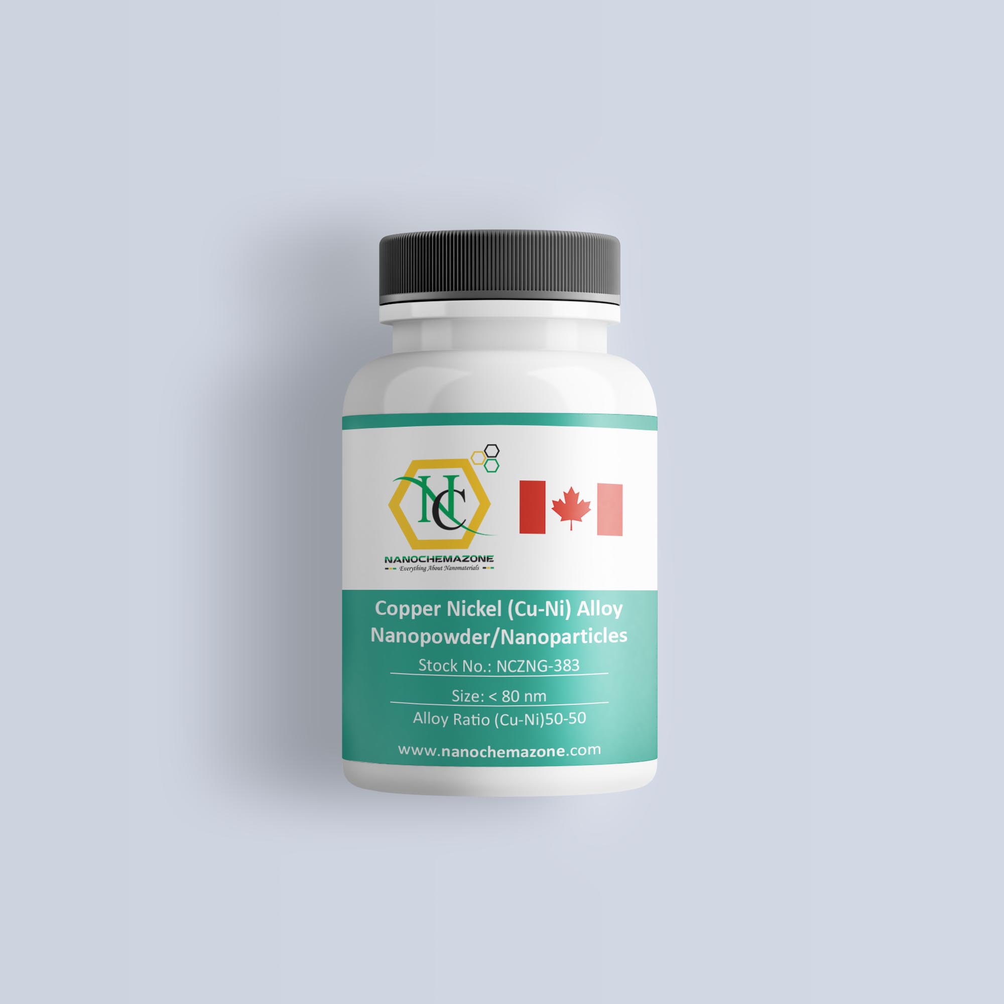
Copper Nickel (Cu-Ni) Alloy Nanopowder/Nanoparticles, Size: < 80 nm

Price range: $76.00 through $307.00
Select options This product has multiple variants. The options may be chosen on the product page

Copper Nickel (Cu-Ni) Alloy Nanopowder/Nanoparticles

Size: < 80 nm

Technical Properties:

Alloy Ratio (Cu-Ni) 50-50
Average Particle Size (nm) 80

Properties, Storage and Cautions:

Cu-Ni alloy nanoparticles are highly reactive, therefore it should be handled with care and rapid moves, vibrations should be avoided. The powder should be kept away from sunlight, any kind of heating, moisture and impacts. Coagulation of the particles is a serious problem, so, the powder should be sealed under vacuum and should be kept in cool and dry conditions. Air contact should be avoided.

Applications:

Cu-Ni alloy is known with its good machinability and resistance to corrosion. It is used in heat exchangers, fittings, pumps, cooling systems, power plants, coins, mechanical and electrical equipment, bullet jackets etc.  

Copper Nickel (Cu-Ni) Alloy Nanopowder/Nanoparticles, Size: < 80 nm

Price range: $76.00 through $307.00
Select options This product has multiple variants. The options may be chosen on the product page
1 gram/67 €  
5 grams/271 €                       
Please contact us for quotes on larger quantities !!!

Copper Nickel (Cu-Ni) Alloy Nanopowder/Nanoparticles

Size: < 80 nm

Technical Properties:

Alloy Ratio (Cu-Ni) 50-50
Average Particle Size (nm) 80

Properties, Storage and Cautions:

Cu-Ni alloy nanoparticles are highly reactive, therefore it should be handled with care and rapid moves, vibrations should be avoided. The powder should be kept away from sunlight, any kind of heating, moisture and impacts. Coagulation of the particles is a serious problem, so, the powder should be sealed under vacuum and should be kept in cool and dry conditions. Air contact should be avoided.

Applications:

Cu-Ni alloy is known with its good machinability and resistance to corrosion. It is used in heat exchangers, fittings, pumps, cooling systems, power plants, coins, mechanical and electrical equipment, bullet jackets etc.

Titanium Diboride (TiB2) Nanopowder/Nanoparticles, Purity: 99%, Size: 62 nm

Price range: $76.00 through $305.00
Select options This product has multiple variants. The options may be chosen on the product page
1 gram/67 € 5 grams/269 €                                        
Please contact us for quotes on larger quantities!

Titanium Diboride (TiB2) Nanopowder/Nanoparticles

Purity: 99%, Size: 62 nm

Storage Condition:

Titanium diboride nanoparticles should be sealed in vacuum and stored in cool and dry room. It should not be exposure to air and avoid stress.

Applications:

Titanium boride nanoparticles is used in hard materials such as ceramic cutting tools, sandblasting nozzles, and metal wortles. It is also used in making armor protection materials. Titanium boride nanoparticles is used as a composite material. It is used in electrical conductivity composite materials and in multi element composite materials.

Vanadium Carbide (VC) Nanopowder/Nanoparticles, Purity: 99.95%, Size: 550-750 nm, Cubic

Price range: $76.00 through $461.00
Select options This product has multiple variants. The options may be chosen on the product page
5 grams/67 € 25 grams/133 € 100 grams/407 €
Please contact us for quotes on larger quantities !!!

Vanadium Carbide (VC) Nanopowder/Nanoparticles

Purity: 99.95%, Size: 550-750 nm, Cubic

Applications:

Vanadium carbide nanoparticles is an extremely hard refractory ceramic material. It is used in cutting tools and tool bits. It also has good high temperature property and chemical stability. It is used as an additive to tungsten carbides in order to fine the carbide crystals to improve the cermet properties.

Nickel (III) Oxide (Ni2O3) Nanopowder/Nanoparticles, Purity: 99.95+ %, Size: 40 nm

Price range: $76.00 through $1,123.00
Select options This product has multiple variants. The options may be chosen on the product page
25 grams/68 € 100 grams/185 € 500 grams/680 € 1 kg/995 €
Please contact us for quotes on larger quantities !!!

Nickel (III) Oxide (Ni2O3) Nanopowder/Nanoparticles

Purity: 99.95+ %, Size: 40 nm

Technical Properties:

Purity (%) 99.95+
Color black-dark gray
Average Particle Size (nm) 40
Specific Surface Area (m2/g) 40-60
Bulk Density (g/cm3) 0.38 g/cm3
True Density (g/cm3) 4.84 g/cm3
Elemental Analysis (wt %) Ni2O3 Co Pb Fe Cu Ca
99.95 <0.014 0.01 0.028 0.01 0.035

ni2o3.png Applications:

Nickel oxide nanoparticles is widely used in different materials. It is used in preparation of nickel cermet for the anode layer of solid oxide fuel cells. It is used in nanowires, nanofibers, and specific alloys. It is used in ceramic structures, electrochromic coatings, plastics, and textiles. Nickel oxide nanoparticles  is used in active optical filters, and automotive rear view mirrors aith adjustable reflectance. It is also used to make energy efficient smart windows with sdjustable absorption and reflectance.

Prime Si+SiO2 Wafer (wet), Size: 4”, Orientation: (111), Phosphor Doped, Resistivity: 1 – 10 (ohm.cm), 1-Side Polished, Thickness: 525 ± 25 μm, Coating 1000 nm

Price range: $76.00 through $1,182.00
Select options This product has multiple variants. The options may be chosen on the product page
1 piece/69 € 5 pieces/245 € 25 pieces/1065 € Please contact us for quotes on larger quantities !!! 

Prime Si+SiO2 Wafer (wet)

Size: 4”, Orientation: (111), Phosphor Doped, 1-Side Polished, Thickness: 525 ± 25 μm, Coating 1000 nm

Technical Properties:

Quality Prime
Materials Si + SiO2 (wet)
Size (inch) 4”
Orientation (111)
Coating 1000 nm
Thickness (μm) 525 ± 25
Doping Phosphor
Resistivity (ohm.cm) 1-10
Polished One Side
Silicon dioxide wafer – also referred as thermal oxide wafer- is produced at elevated temperatures. Thermal oxide is normally grown in a horizontal tube furnace, at temperature range from 900°C ~ 1200°C. Thermal oxide is a kind of "grown" oxide layer , compared to CVD deposited oxide layer , it has a higher uniformity, and higher dielectric strength , it is an excellent dielectric layer as an insulator. In most silicon-based devices, thermal oxide layer plays an important role to pacify the silicon surface to act as doping barriers and as surface dielectrics. It allows a very good thickness uniformity and purity. Therefore, this is the preferred way to produce high quality thin silicon oxide layers. Thicker oxide layers are typically produced by wet oxidation where the growth rate is significantly increased.

Prime Si+Si3N4 Wafer, Size: 4”, Orientation: (100), Arsenic Doped, Resistivity: 0,001-0,005 (ohm.cm), 1 Side Polished, Thickness: 525± 25 μm, Coating 450 nm

Price range: $76.00 through $1,599.00
Select options This product has multiple variants. The options may be chosen on the product page
1 piece/69 € 5 pieces/310 € 25 pieces/1450 € Please contact us for quotes on larger quantities !!! 

Prime Si+Si3N4 Wafer

Size: 4”, Orientation: (100), Arsenic Doped, Thickness: 525± 25 μm

Technical Properties:

Quality Prime
Materials Si+Si3N4
Size (inch) 4”
Orientation (100)
Coating 450 nm
Thickness (μm) 525± 25
Doping Arsenic
Resistivity (ohm.cm) 0,001-0,005
Polished One Side
  Silicon nitride (Si3N4,SiN) offers excellent mechanical and thermal stability. It is commonly used for hard masks, as a dielectric material, or as a passivation layer. Silicon nitride is very hard by nature and has good thermal shock resistance and oxidation resistance. Silicon Nitride has good high temperature strength, creep resistance and oxidation resistance. Silicon Nitride's low thermal expansion coefficient gives good thermal shock resistance.

Fused Silica Wafer, Size: 6”, 2-Side Polished, Thickness: 700 ± 25 μm

Price range: $76.00 through $1,620.00
Select options This product has multiple variants. The options may be chosen on the product page
Fused Silica Wafer Size: 6”, 2-Side Polished, Thickness: 700 ± 25 μm Technical Properties: Quality Prime Materials Fused Silica Size

Fused Silica Wafer, Size: 4”, 2-Side Polished, Thickness: 500 ± 25 μm

Price range: $76.00 through $1,620.00
Select options This product has multiple variants. The options may be chosen on the product page
Fused Silica Wafer Size: 4”, 2-Side Polished, Thickness: 500 ± 25 μm Technical Properties: Quality Prime Materials Fused Silica Size

Prime Si+SiO2 Wafer (wet), Size: 4”, Orientation: (111), Phosphor Doped, Resistivity: 1 – 10 (ohm.cm), 1-Side Polished, Thickness: 525 ± 25 μm, Coating 1000 nm

Price range: $76.00 through $1,278.00
Select options This product has multiple variants. The options may be chosen on the product page
Prime Si+SiO2 Wafer (wet) Size: 4”, Orientation: (111), Phosphor Doped, 1-Side Polished, Thickness: 525 ± 25 μm, Coating 1000 nm

Prime Si+SiO2 Wafer (wet), Size: 4”, Orientation: (100), Boron Doped, Resistivity: 0.001 – 0.01 (ohm.cm), 1-Side Polished, Thickness: 525 ± 25 μm, Coating 500 nm

Price range: $76.00 through $1,158.00
Select options This product has multiple variants. The options may be chosen on the product page
Prime Si+SiO2 Wafer (wet) Size: 4”, Orientation: (100), Boron Doped, 1-Side Polished, Thickness: 525 ± 25 μm, Coating 500 nm

Prime FZ-Si Wafer, Size: 4”, Orientation: (100), Boron Doped, Resistivity: 2000 – 4000 (ohm.cm), 1-Side Polished, Thickness: 300 ± 10 μm

Price range: $76.00 through $1,158.00
Select options This product has multiple variants. The options may be chosen on the product page
Prime FZ-Si Wafer Size: 4”, Orientation: (100), Boron Doped, 1-Side Polished, Thickness: 300 ± 10 μm Technical Properties: Quality Prime

Borosilicate Wafer, Size: 4”, 2-Side polished, Thickness: 200 ± 20 μm

Price range: $76.00 through $1,128.00
Select options This product has multiple variants. The options may be chosen on the product page
Boroslicate Wafer Size: 4”, 2-Side polished, Thickness: 200 ± 20 μm Technical Properties: Materials Borosilicate Size (inch) 4” Orientation Coating

Silicon (Si) Sputtering Targets, undoped, Purity: 99.999%, Size: 1”, Thickness: 0.125”

$76.00

Applications of Sputtering Targets;

Film deposition is accomplished using sputtering targets. A technique for sputtering thin films is called "deposition made by sputter targets," which entails eroding material from a "target" source onto a "substrate" like a silicon wafer. Etching of the target is done using semiconductor sputtering targets. When selectivity is not an issue and a high degree of etching anisotropy is required, sputter etching is the method of choice. By removing the target material through etching, sputter targets are also utilized for investigation. In secondary ion spectroscopy (SIMS), one example is when the target material is sputtered at a steady pace. Mass spectrometry is used to quantify the concentration and identity of spewed atoms as the target is sputtered.

The target material's composition may be ascertained and even very low concentrations of contaminants can be found with the aid of the sputtering target.

There is also an application area for sputtering targets in space. One type of space weathering that alters the chemical and physical characteristics of airless worlds like the Moon and asteroids is sputtering.

Tungsten (W) Sputtering Targets, Purity: 99.95%, Size: 1”, Thickness: 0.125”

$76.00

Applications of Sputtering Targets;

Film deposition is accomplished using sputtering targets. A technique for sputtering thin films is called "deposition made by sputter targets," which entails eroding material from a "target" source onto a "substrate" like a silicon wafer. Etching of the target is done using semiconductor sputtering targets. When selectivity is not an issue and a high degree of etching anisotropy is required, sputter etching is the method of choice. By removing the target material through etching, sputter targets are also utilized for investigation. In secondary ion spectroscopy (SIMS), one example is when the target material is sputtered at a steady pace. Mass spectrometry is used to quantify the concentration and identity of spewed atoms as the target is sputtered.

The target material's composition may be ascertained and even very low concentrations of contaminants can be found with the aid of the sputtering target.

There is also an application area for sputtering targets in space. One type of space weathering that alters the chemical and physical characteristics of airless worlds like the Moon and asteroids is sputtering.

Boron Nitride Powder (BN, hexagonal, 99+%, 3~4um)

Price range: $76.00 through $213.00
Select options This product has multiple variants. The options may be chosen on the product page
$76/100g
$213/500g

Product 

Boron Nitride Powder (BN, hexagonal, 99+%, 3~4um)

CAS No.

10043-11-5

Appearance

Powder

Purity

≥99%,  ≥99.9%,  ≥95%

(Other purities are also available)

APS

 3~4um (Size Can be customized), Ask for other available size ranges.

Ingredient

N/A

Molecular Weight

24.82 g/mol

Melting Point

>2,973 °C (sublimes without melting)

Boiling Point

Sublimes at ~2,973 °C

Density

~2.1–2.3 g/cm³

Product Codes

NCZ-1104K

Indium Tin Oxide Nanoparticles (ITO, Yellow, In2O3:SnO2=95:5, 99.99%, 20-70 nm)

Price range: $76.00 through $287.00
Select options This product has multiple variants. The options may be chosen on the product page
$76/5g
$126/25g
$287/100g

Product 

Indium Tin Oxide Nanoparticles (ITO, Yellow, In2O3:SnO2=95:5, 99.99%, 20-70 nm)

CAS No.

1312-43-2

Appearance

Powder

Purity

≥99%,  ≥99.9%,  ≥95%

(Other purities are also available)

APS

20-70 nm (Size Can be customized), Ask for other available size ranges.

Ingredient

N/A

Molecular Weight

~277.6 g/mol

Melting Point

~1,800 °C (depends on exact stoichiometry)

Boiling Point

Decomposes

Density

~7.1 g/cm³

Product Codes

NCZ-1141K

Indium Tin Oxide Nanoparticles/ Nanopowder( ITO, yellow, In2O3:SnO2=90:10, 99.99%, 20~70nm)

Price range: $76.00 through $287.00
Select options This product has multiple variants. The options may be chosen on the product page
$76/5g
$126/25g
$287/100g

Product 

Indium Tin Oxide Nanoparticles/ Nanopowder( ITO, yellow, In2O3:SnO2=90:10, 99.99%, 20~70nm)

CAS No.

1312-43-2

Appearance

Powder

Purity

≥99%,  ≥99.9%,  ≥95%

(Other purities are also available)

APS

20-70 nm (Size Can be customized), Ask for other available size ranges.

Ingredient

N/A

Molecular Weight

~277.6 g/mol

Melting Point

~1,800 °C (depends on exact stoichiometry)

Boiling Point

Decomposes

Density

~7.1 g/cm³

Product Codes

NCZ-1140K

Graphene NMP Dispersion, Purity: 99.5%, Graphene: 1,0 wt%

Price range: $77.00 through $531.00
Select options This product has multiple variants. The options may be chosen on the product page
Graphene NMP Dispersion, Purity: 99.5%, Graphene: 1,0 wt%
Graphene Purity (%) 99,5
Graphene Thickness (nm) 0,6-1,2
Diameter (µm) 2,0-12,0
Appearance Black Liquid
Concentration (wt%) 1,0 (mg/ml)
Specific Surface Area (m2/g) 600-1200
Elemental Analysis (%) C            O 99,6    <0,4
Surfactant                                                                                                           YES

Boron (B) Nanopowder/Nanoparticles, Purity: 99.55+%, Size: 450 nm

Price range: $77.00 through $1,132.00
Select options This product has multiple variants. The options may be chosen on the product page

Boron (B) Nanopowder/Nanoparticles

Purity: 99.55+%, Size: 450 nm

Technical Properties:

Color brown-black
Crystal Structure amorphous
Hardness 9,5 (Mohs Scale)
Tmelting (oC) 2400
Tboiling (oC) 2700
Average Particle Size (nm) 450
Elemental Analysis B O S C N Mg Others
99.55 0.2 0.06 0.04 0.04 0.04 0.01

High Purity Natural Graphite Nanopowder/Nanoparticles for Li-ion Battery, Purity: 99.99+%, Size: 30 nm

Price range: $77.00 through $1,128.00
Select options This product has multiple variants. The options may be chosen on the product page

High Purity Natural Graphite Nanopowder/Nanoparticles for Li-ion Battery

Purity: 99.99+%, Size: 30 nm

Technical Properties:

  Nanografi Particle Size (nm)    Purity (%)   BET (m2 /g) Bulk Density (g/cm3) True Density (g/cm3) Particle Morphology    Color
 NG08BE0305          30 >99.99 195 0.18 2

Boron (B) Micron Powder, Purity: 99 %, Size: -325 mesh, Amorphous

Price range: $77.00 through $654.00
Select options This product has multiple variants. The options may be chosen on the product page
  25 grams/68 € 100 grams/134 € 500 grams/323 € 1000 grams/578 €
Please contact us for quotes on larger quantities !!!

Boron (B) Micron Powder

Purity: 99 %, Size: 325 mesh, Amorphous

Technical Properties:

 
PURITY

99%

PARTICLE SIZE

-325 Mesh

CAS

7440-42-8

BOILING POINT

2100 °C

MELTING POINT

2600 °C

ELECTRIC RESISTIVITY

4 x 10 ⁶ microhm-cm

MOHS HARDNESS @ 20ºC

9.3

FORM  

Powder

APPLICATIONS

Aerospace, Ceramics, Fuel Source, Nuclear


Prime Si+Si3N4 Wafer, Size: 4”, Orientation: (100), Boron Doped, Resistivity: 1-10 (ohm.cm), 2 Side Polished, Thickness: 525± 25 μm, Coating 150 nm

Price range: $77.00 through $1,560.00
Select options This product has multiple variants. The options may be chosen on the product page
Prime Si+Si3N4 Wafer Size: 4”, Orientation: (100), Boron Doped, Thickness: 525± 25 μm, Coating 150 nm Technical Properties: Quality Prime

Indium Oxide Nanoparticles/ Nanopowder (In2O3, 99.99+%, 20~70nm)

Price range: $77.00 through $415.00
Select options This product has multiple variants. The options may be chosen on the product page
$77/5g
$185/25g
$415/100g

Product 

Indium Oxide Nanoparticles/ Nanopowder (In2O3, 99.99+%, 20~70nm)

CAS No.

1312-43-2

Appearance

Powder

Purity

≥99%,  ≥99.9%,  ≥95%

(Other purities are also available)

APS

20~70nm (Size Can be customized), Ask for other available size ranges.

Ingredient

N/A

Molecular Weight

 277.64 g/mol

Melting Point

 ~1,910 °C

Boiling Point

~3,400 °C (sublimes/decomposes)

Density

~7.18 g/cm³

Product Codes

NCZ-1144K

1 kg, 75-85 um Alpha Aluminum Oxide (Alumina) Al2O3 Powder 99.9% 3N

$77.00
Product 1 kg, 75-85 um Alpha Aluminum Oxide (Alumina) Al2O3 Powder 99.9% 3N
CAS No. 1344-28-1
Appearance White
Purity ≥99%,  ≥99.9%,  ≥95%(Other purities are also available)
APS 1 - 2µm (Size Can be customized), Ask for other available size range.
Ingredient Al2O3
Molecular Weight 101.96 g/mol
Melting Point N/A
Boiling Point N/A
Density 3.987 g/cm3
Product Codes NCZ-110I

99.9% 3N 1-5 um Alpha Aluminum Oxide (Alumina) Al2O3 Powder, 500 g

$77.00
Product 99.9% 3N 1-5 um Alpha Aluminum Oxide (Alumina) Al2O3 Powder, 500 g
CAS No. 1344-28-1
Appearance White crystalline
Purity ≥99%,  ≥99.9%,  ≥95%(Other purities are also available)
APS 1-5um (Size Can be customized),  Ask for other available size range.
Ingredient Al2O3
Molecular Weight N/A
Melting Point N/A
Boiling Point N/A
Density 3.95–4.0 g/cm³
Product Codes NCZ-227I
 

Lanthanum (III) Oxide (La2O3) 99.999% 5N Powder

Price range: $77.00 through $359.00
Select options This product has multiple variants. The options may be chosen on the product page
Product Lanthanum (III) Oxide (La2O3) 99.999% 5N Powder
CAS No. 12037-29-5
Appearance White to off-white
Purity ≥99%,  ≥99.9%,  ≥95%(Other purities are also available)
APS 1–10nm (Size Can be customized),  Ask for other available size range.
Ingredient La2O3
Molecular Weight 325.81 g/mol
Melting Point N/A
Boiling Point N/A
Density 6.51 g/cm³
Product Codes NCZ-434I

Copper (Cu) Sputtering Targets, Purity: 99.99%, Size: 1”, Thickness: 0.250′

$77.40

Applications of Sputtering Targets;

Film deposition is accomplished using sputtering targets. A technique for sputtering thin films is called "deposition made by sputter targets," which entails eroding material from a "target" source onto a "substrate" like a silicon wafer. Etching of the target is done using semiconductor sputtering targets. When selectivity is not an issue and a high degree of etching anisotropy is required, sputter etching is the method of choice. By removing the target material through etching, sputter targets are also utilized for investigation. In secondary ion spectroscopy (SIMS), one example is when the target material is sputtered at a steady pace. Mass spectrometry is used to quantify the concentration and identity of spewed atoms as the target is sputtered.

The target material's composition may be ascertained and even very low concentrations of contaminants can be found with the aid of the sputtering target.

There is also an application area for sputtering targets in space. One type of space weathering that alters the chemical and physical characteristics of airless worlds like the Moon and asteroids is sputtering.

(-COOH) Functionalized Double Walled Carbon Nanotubes, Purity: > 65%

Price range: $78.00 through $750.00
Select options This product has multiple variants. The options may be chosen on the product page

(-COOH) Functionalized Double Walled Carbon Nanotubes

Purity: > 65%, Length: 48 µm, black

Double walled carbon nanotubes are especial class of carbon nanotubes, comprise of two nanotubes placed inside one another. Varying degrees of interaction between the two tubes due to the differences in the diameter of the tubes results in unique and interesting optical, mechanical and electronic properties. DWCNTs can be applied in many different areas such as emission displays (FEDs) and field emission transistors (FETs) whereby their impressive properties. For applications requiring the highest quality, We offer Double Walled Carbon Nano Tubes with low prices.

Prime Si+SiO2 Wafer (wet), Size: 4”, Orientation: (100), Boron Doped, Resistivity: 1 – 10 (ohm.cm), 1-Side Polished, Thickness: 525 ± 25 μm, Coating 1500 nm

Price range: $78.00 through $1,237.00
Select options This product has multiple variants. The options may be chosen on the product page
1 piece/71 € 5 pieces/255 € 25 pieces/1115 € Please contact us for quotes on larger quantities !!! 

Prime Si+SiO2 Wafer (wet)

Size: 4”, Orientation: (100), Boron Doped, 1-Side Polished, Thickness: 525 ± 25 μm, Coating 1500 nm

Technical Properties:

Quality Prime
Materials Si + SiO2 (wet)
Size (inch) 4”
Orientation (100)
Coating 1500 nm
Thickness (μm) 525 ± 25
Doping Boron
Resistivity (ohm.cm) 1-10
Polished One Side
Silicon dioxide wafer – also referred as thermal oxide wafer- is produced at elevated temperatures. Thermal oxide is normally grown in a horizontal tube furnace, at temperature range from 900°C ~ 1200°C. Thermal oxide is a kind of "grown" oxide layer , compared to CVD deposited oxide layer , it has a higher uniformity, and higher dielectric strength , it is an excellent dielectric layer as an insulator. In most silicon-based devices, thermal oxide layer plays an important role to pacify the silicon surface to act as doping barriers and as surface dielectrics. It allows a very good thickness uniformity and purity. Therefore, this is the preferred way to produce high quality thin silicon oxide layers. Thicker oxide layers are typically produced by wet oxidation where the growth rate is significantly increased.

Prime Si+Si3N4 Wafer, Size: 4”, Orientation: (100), Boron Doped, Resistivity: 1-10 (ohm.cm), 2 Side Polished, Thickness: 525± 25 μm, Coating 70 nm

Price range: $78.00 through $1,544.00
Select options This product has multiple variants. The options may be chosen on the product page
Prime Si+Si3N4 Wafer Size: 4”, Orientation: (100), Boron Doped, Thickness: 525± 25 μm, Coating 70 nm Technical Properties: Quality Prime

Yttrium Aluminate (Y3Al5O12) Nanopowder/Nanoparticles, Purity: 99.7+%, Size: 25 nm

Price range: $78.00 through $306.00
Select options This product has multiple variants. The options may be chosen on the product page

Applications:

Yttrium Aluminum Oxide nanoparticles has applications in electronic devices. It is used in temperature sensors, P-type transparent conductive films, and counter electrodes. It is used as cathode materials for alkaline batteries. Its optical properties can be used in active optical filters, and automotive rear-view mirrors with adjustable reflectance. It also has applications in the field of catalysis.