Magnesium Oxide (MgO) Sputtering Targets, Purity: 99.95%, Size: 5”, Thickness: 0.125”

$537.00

Applications of Sputtering Targets;

Film deposition is accomplished using sputtering targets. A technique for sputtering thin films is called "deposition made by sputter targets," which entails eroding material from a "target" source onto a "substrate" like a silicon wafer. Etching of the target is done using semiconductor sputtering targets. When selectivity is not an issue and a high degree of etching anisotropy is required, sputter etching is the method of choice. By removing the target material through etching, sputter targets are also utilized for investigation. In secondary ion spectroscopy (SIMS), one example is when the target material is sputtered at a steady pace. Mass spectrometry is used to quantify the concentration and identity of spewed atoms as the target is sputtered.

By helping of the sputtering target, the composition of the target material may be evaluated and even extremely tiny amounts of contaminants are recognized.

There is also an application area for sputtering targets in space. One type of space weathering that alters the chemical and physical characteristics of airless worlds like the Moon and asteroids is sputtering.

Lanthanum Calcium Manganate (La0.7Ca0.3MnO3) Sputtering Targets, Purity: 99.9%, Size: 4”, Thickness: 0.250”

$536.00

Product 

Lanthanum Calcium Manganate (La0.7Ca0.3MnO3) Sputtering Targets, Purity: 99.9%, Size: 4'', Thickness: 0.250''

CAS No.

123273‑09‑6

Appearance

Powder

Purity

≥99%,  ≥99.9%,  ≥95%

(Other purities are also available)

APS

 N/A (Size Can be customized), Ask for other available size ranges.

Ingredient

N/A

Molecular Weight

 ~313.9 g/mol

Melting Point

 ~1,550 °C (approximate; ceramic decomposition likely above)

Boiling Point

N/A

Density

 ~5.3 g/cm³ @ room temp

Product Codes

NCZ-2151K

Zinc Oxide (ZnO) with Alumina Sputtering Targets, Purity: 99.99%, Size: 4”, Thickness: 0.125”

$536.00

Applications of Sputtering Targets;

Film deposition is accomplished using sputtering targets. A technique for sputtering thin films is called "deposition made by sputter targets," which entails eroding material from a "target" source onto a "substrate" like a silicon wafer. Etching of the target is done using semiconductor sputtering targets. When selectivity is not an issue and a high degree of etching anisotropy is required, sputter etching is the method of choice. By removing the target material through etching, sputter targets are also utilized for investigation. In secondary ion spectroscopy (SIMS), one example is when the target material is sputtered at a steady pace. Mass spectrometry is used to quantify the concentration and identity of spewed atoms as the target is sputtered.

The target material's composition may be ascertained and even very low concentrations of contaminants can be found with the aid of the sputtering target.

There is also an application area for sputtering targets in space. One type of space weathering that alters the chemical and physical characteristics of airless worlds like the Moon and asteroids is sputtering.

Boron Carbide (B4C) Sputtering Targets, Purity: 99.5%, Size: 8”, Thickness: 0.125”

$536.00

Applications of Sputtering Targets;

Film deposition is accomplished using sputtering targets. A technique for sputtering thin films is called "deposition made by sputter targets," which entails eroding material from a "target" source onto a "substrate" like a silicon wafer. Etching of the target is done using semiconductor sputtering targets. When selectivity is not an issue and a high degree of etching anisotropy is required, sputter etching is the method of choice. By removing the target material through etching, sputter targets are also utilized for investigation. In secondary ion spectroscopy (SIMS), one example is when the target material is sputtered at a steady pace. Mass spectrometry is used to quantify the concentration and identity of spewed atoms as the target is sputtered.

The target material's composition may be ascertained and even very low concentrations of contaminants can be found with the aid of the sputtering target.

There is also an application area for sputtering targets in space. One type of space weathering that alters the chemical and physical characteristics of airless worlds like the Moon and asteroids is sputtering.

Aluminum Oxide (Al2O3) Sputtering Targets, Purity: 99.999%, Size: 2”, Thickness: 0.250”

$536.00

Applications of Sputtering Targets;

Film deposition is accomplished using sputtering targets. A technique for sputtering thin films is called "deposition made by sputter targets," which entails eroding material from a "target" source onto a "substrate" like a silicon wafer. Etching of the target is done using semiconductor sputtering targets. When selectivity is not an issue and a high degree of etching anisotropy is required, sputter etching is the method of choice. By removing the target material through etching, sputter targets are also utilized for investigation. In secondary ion spectroscopy (SIMS), one example is when the target material is sputtered at a steady pace. Mass spectrometry is used to quantify the concentration and identity of spewed atoms as the target is sputtered. With the sputtering target's assistance, the

It is possible to identify the target material and even detect incredibly tiny impurity amounts.

There is also an application area for sputtering targets in space. One type of space weathering that alters the chemical and physical characteristics of airless worlds like the Moon and asteroids is sputtering.

With the chemical formula Al2O3, aluminum oxide is a compound made of aluminum and oxygen. Because of its high melting point, Al2O3 is useful as a refractory material and as an abrasive due to its hardness, as well as for the production of aluminum metal.

Silver (Ag) Sputtering Targets, Purity: 99.99%, Size: 3”, Thickness: 0.250”

$534.00

Applications of Sputtering Targets;

Film deposition is accomplished using sputtering targets. A technique for sputtering thin films is called "deposition made by sputter targets," which entails eroding material from a "target" source onto a "substrate" like a silicon wafer. Etching of the target is done using semiconductor sputtering targets. When selectivity is not an issue and a high degree of etching anisotropy is required, sputter etching is the method of choice. By removing the target material through etching, sputter targets are also utilized for investigation. In secondary ion spectroscopy (SIMS), one example is when the target material is sputtered at a steady pace. Mass spectrometry is used to quantify the concentration and identity of spewed atoms as the target is sputtered.

The target material's composition may be ascertained and even very low concentrations of contaminants can be found with the aid of the sputtering target.

There is also an application area for sputtering targets in space. One type of space weathering that alters the chemical and physical characteristics of airless worlds like the Moon and asteroids is sputtering.

Lanthanum Calcium Manganate (La0.7Ca0.3MnO3) Sputtering Targets, Purity: 99.9%, Size: 2”, Thickness: 0.125”

$534.00

Applications of Sputtering Targets;

Film deposition is accomplished using sputtering targets. A technique for sputtering thin films is called "deposition made by sputter targets," which entails eroding material from a "target" source onto a "substrate" like a silicon wafer. Etching of the target is done using semiconductor sputtering targets. When selectivity is not an issue and a high degree of etching anisotropy is required, sputter etching is the method of choice. By removing the target material through etching, sputter targets are also utilized for investigation. In secondary ion spectroscopy (SIMS), one example is when the target material is sputtered at a steady pace. Mass spectrometry is used to quantify the concentration and identity of spewed atoms as the target is sputtered.

The target material's composition may be ascertained and even very low concentrations of contaminants can be found with the aid of the sputtering target.

There is also an application area for sputtering targets in space. One type of space weathering that alters the chemical and physical characteristics of airless worlds like the Moon and asteroids is sputtering.

Yttrium (Y) Sputtering Targets, Purity: 99.9%, Size: 2”, Thickness: 0.250”

$533.00

Product 

Yttrium (Y) Sputtering Targets, Purity: 99.9%, Size: 2'', Thickness: 0.250''

CAS No.

7440-65-5

Appearance

Powder

Purity

≥99%,  ≥99.9%,  ≥95%

(Other purities are also available)

APS

N/A  (Size Can be customized), Ask for other available size ranges.

Ingredient

N/A

Molecular Weight

88.91 g/mol

Melting Point

1522 °C

Boiling Point

3338 °C

Density

4.47 g/cm³

Product Codes

NCZ-1520K

Lanthanum Manganate (LaMnO3) Sputtering Targets, Purity: 99.9%, Size: 2”, Thickness: 0.125”

$532.00

Applications of Sputtering Targets;

Film deposition is accomplished using sputtering targets. A technique for sputtering thin films is called "deposition made by sputter targets," which entails eroding material from a "target" source onto a "substrate" like a silicon wafer. Etching of the target is done using semiconductor sputtering targets. When selectivity is not an issue and a high degree of etching anisotropy is required, sputter etching is the method of choice. By removing the target material through etching, sputter targets are also utilized for investigation. In secondary ion spectroscopy (SIMS), one example is when the target material is sputtered at a steady pace. Mass spectrometry is used to quantify the concentration and identity of spewed atoms as the target is sputtered.

The target material's composition may be ascertained and even very low concentrations of contaminants can be found with the aid of the sputtering target.

There is also an application area for sputtering targets in space. One type of space weathering that alters the chemical and physical characteristics of airless worlds like the Moon and asteroids is sputtering.

Barium Titanate (BaTiO3) Sputtering Targets, Purity: 99.99%, Size: 1”, Thickness: 0.250”

$532.00

Applications of Sputtering Targets;

Film deposition is accomplished using sputtering targets. A technique for sputtering thin films is called "deposition made by sputter targets," which entails eroding material from a "target" source onto a "substrate" like a silicon wafer. Etching of the target is done using semiconductor sputtering targets. When selectivity is not an issue and a high degree of etching anisotropy is required, sputter etching is the method of choice. By removing the target material through etching, sputter targets are also utilized for investigation. In secondary ion spectroscopy (SIMS), one example is when the target material is sputtered at a steady pace. Mass spectrometry is used to quantify the concentration and identity of spewed atoms as the target is sputtered. With the sputtering target's assistance, the

It is possible to identify the target material and even detect incredibly tiny impurity amounts.

There is also an application area for sputtering targets in space. One type of space weathering that alters the chemical and physical characteristics of airless worlds like the Moon and asteroids is sputtering.

Formulated as BaTiO3, barium titanate is an inorganic substance. When formed as big crystals, barium titanate is clear and has a white powdery appearance. It is a ferroelectric ceramic material with piezoelectric and photorefractive characteristics. Titanate of barium sputtering

Indium (In) Sputtering Targets, Purity: 99.999%, Size: 3”, Thickness: 0.125”

$531.00

Product 

Indium (In) Sputtering Targets, Purity: 99.999%, Size: 3'', Thickness: 0.125''

CAS No.

 7440-74-6

Appearance

Powder

Purity

≥99%,  ≥99.9%,  ≥95%

(Other purities are also available)

APS

 N/A (Size Can be customized), Ask for other available size ranges.

Ingredient

N/A

Molecular Weight

114.82 g/mol

Melting Point

 156.6 °C

Boiling Point

 2,072 °C

Density

 7.31 g/cm³

Product Codes

NCZ-2226K

Silicon (Si) Sputtering Targets, N-type, Purity: 99.999%, Size: 8”, Thickness: 0.250”

$531.00

Product 

Silicon (Si) Sputtering Targets, N-type, Purity: 99.999%, Size: 8'', Thickness: 0.250''

CAS No.

7440-21-3

Appearance

Powder

Purity

≥99%,  ≥99.9%,  ≥95%

(Other purities are also available)

APS

N/A  (Size Can be customized), Ask for other available size ranges.

Ingredient

N/A

Molecular Weight

28.0855 g/mol

Melting Point

 1,414 °C

Boiling Point

3,265 °C

Density

 2.33 g/cm³

Product Codes

NCZ-1754K

Vanadium Oxide (V2O5) Sputtering Targets, Purity: 99.9%, Size: 4”, Thickness: 0.125”

$531.00

Applications of Sputtering Targets;

Film deposition is accomplished using sputtering targets. A technique for sputtering thin films is called "deposition made by sputter targets," which entails eroding material from a "target" source onto a "substrate" like a silicon wafer. Etching of the target is done using semiconductor sputtering targets. When selectivity is not an issue and a high degree of etching anisotropy is required, sputter etching is the method of choice. By removing the target material through etching, sputter targets are also utilized for investigation. In secondary ion spectroscopy (SIMS), one example is when the target material is sputtered at a steady pace. Mass spectrometry is used to quantify the concentration and identity of spewed atoms as the target is sputtered.

The target material's composition may be ascertained and even very low concentrations of contaminants can be found with the aid of the sputtering target.

There is also an application area for sputtering targets in space. One type of space weathering that alters the chemical and physical characteristics of airless worlds like the Moon and asteroids is sputtering.

Antimony (Sb) Sputtering Targets, elastomer, Purity: 99.999%, Size: 2”, Thickness: 0.125”

$531.00

Applications of Sputtering Targets;

Film deposition is accomplished using sputtering targets. A technique for sputtering thin films is called "deposition made by sputter targets," which entails eroding material from a "target" source onto a "substrate" like a silicon wafer. Etching of the target is done using semiconductor sputtering targets. When selectivity is not an issue and a high degree of etching anisotropy is required, sputter etching is the method of choice. By removing the target material through etching, sputter targets are also utilized for investigation. In secondary ion spectroscopy (SIMS), one example is when the target material is sputtered at a steady pace. When the target shatters,

Mass spectrometry measures the concentration and identity of sputtered atoms. The target material's composition may be ascertained and even very low concentrations of contaminants can be found with the aid of the sputtering target.

There is also an application area for sputtering targets in space. One type of space weathering that alters the chemical and physical characteristics of airless worlds like the Moon and asteroids is sputtering.

Group 15 of the periodic table contains antimony (Sb), which shares an atomic number of 51 with bismuth and arsenic. It gleams with a metallic sheen.

bluish-white in color. Despite not having the same reputation as a poison, antimony shares many of the same chemical characteristics as arsenic. Its average natural abundance in the earth's crust is 0.2 to 0.5 parts per million. Antimony sputtering targets can be utilized to create fire-retardant coatings since antimony has excellent fire retardance properties. Antimony sputtering targets can also be utilized for optoelectronic devices such as solar cells, laser diodes, photodiodes, and LEDs.

Manganese (Mn) Sputtering Targets, indium, Purity: 99.95%, Size: 1”, Thickness: 0.125”

$530.00

Product 

Manganese (Mn) Sputtering Targets, indium, Purity: 99.95%, Size: 1'', Thickness: 0.125''

CAS No.

 7439-96-5

Appearance

Powder

Purity

≥99%,  ≥99.9%,  ≥95%

(Other purities are also available)

APS

 N/A (Size Can be customized), Ask for other available size ranges.

Ingredient

N/A

Molecular Weight

54.93804 g/mol

Melting Point

 1,246 °C

Boiling Point

 2,061 °C

Density

 7.21 g/cm³

Product Codes

NCZ-1944K

Tin Oxide (SnO2) Sputtering Targets, Purity: 99.99%, Size: 3”, Thickness: 0.250”

$530.00

Applications of Sputtering Targets;

Film deposition is accomplished using sputtering targets. A technique for sputtering thin films is called "deposition made by sputter targets," which entails eroding material from a "target" source onto a "substrate" like a silicon wafer. Etching of the target is done using semiconductor sputtering targets. When selectivity is not an issue and a high degree of etching anisotropy is required, sputter etching is the method of choice. By removing the target material through etching, sputter targets are also utilized for investigation. In secondary ion spectroscopy (SIMS), one example is when the target material is sputtered at a steady pace. Mass spectrometry is used to quantify the concentration and identity of spewed atoms as the target is sputtered.

The target material's composition may be ascertained and even very low concentrations of contaminants can be found with the aid of the sputtering target.

There is also an application area for sputtering targets in space. One type of space weathering that alters the chemical and physical characteristics of airless worlds like the Moon and asteroids is sputtering.

Yttrium (Y) Sputtering Targets, Purity: 99.9%, Size: 3”, Thickness: 0.125”

$528.00

Applications of Sputtering Targets;

  • Sputtering targets is used for film deposition. The deposition made by sputter targets is a method of depositing thin films by sputtering that involves eroding material from a "target" source onto a "substrate" such as  a silicon wafer.
  • Semiconductor sputtering targets is used to etch the target. Sputter etching is chosen in cases where a high degree of etching anisotropy is needed and selectivity is not a concern.
  • Sputter targets is also used for analysis by etching away the target material.
One of the example occurs in secondary ion spectroscopy (SIMS), where the target sample is sputtered at a constant rate. As the target is sputtered, the concentration and identity of sputtered atoms are measured using mass spectrometry. By helping of the sputtering target, the composition of the target material can be determined and even extremely low concentrations of impurities are detected. Sputtering target has also application area in space. Sputtering is one of the forms of space weathering, a process that changes the physical and chemical properties of airless bodies, such as asteroids and the Moon.

Cobalt Iron Boron (Co-Fe-B) Sputtering Targets, Purity: 99.95%, Size: 2”, Thickness: 0.125”

$526.00

Product 

Cobalt Iron Boron (Co-Fe-B) Sputtering Targets, Purity: 99.95%, Size: 2'', Thickness: 0.125''

CAS No.

N/A

Appearance

Powder

Purity

≥99%,  ≥99.9%,  ≥95%

(Other purities are also available)

APS

 N/A (Size Can be customized), Ask for other available size ranges.

Ingredient

N/A

Molecular Weight

 ~135.943 g/mol

Melting Point

N/A

Boiling Point

N/A

Density

0.986 g/cm³ (SAM — verify via COA due to low value)

Product Codes

NCZ-2280K

Aluminum Oxide (Al2O3) Sputtering Target

Price range: $174.00 through $526.00
Select options This product has multiple variants. The options may be chosen on the product page

Product 

Aluminum Oxide (Al2O3) Sputtering Target

CAS No.

1344-28-1

Appearance

Powder

Purity

≥99%,  ≥99.9%,  ≥95%

(Other purities are also available)

APS

 NA (Size Can be customized), Ask for other available size ranges.

Ingredient

N/A

Molecular Weight

101.96 g/mol

Melting Point

2,072 °C

Boiling Point

 ~2,977 °C

Density

 3.95 – 4.1 g/cm³

Product Codes

NCZ-1365K

Niobium Oxide (Nb2O5) Sputtering Target

Price range: $115.00 through $526.00
Select options This product has multiple variants. The options may be chosen on the product page

Product 

Niobium Oxide (Nb2O5) Sputtering Target

CAS No.

1313-96-8

Appearance

Powder

Purity

≥99%,  ≥99.9%,  ≥95%

(Other purities are also available)

APS

 NA (Size Can be customized), Ask for other available size ranges.

Ingredient

N/A

Molecular Weight

265.81 g/mol

Melting Point

~1,510 °C

Boiling Point

N\A

Density

~4.6–4.9 g/cm³

Product Codes

NCZ-1322K

Titanium Dioxide (TiO2) Sputtering Targets, Purity: 99.9%, Size: 4”, Thickness: 0.125”, Grey to Black

$526.00

Applications of Sputtering Targets;

Film deposition is accomplished using sputtering targets. A technique for sputtering thin films is called "deposition made by sputter targets," which entails eroding material from a "target" source onto a "substrate" like a silicon wafer. Etching of the target is done using semiconductor sputtering targets. When selectivity is not an issue and a high degree of etching anisotropy is required, sputter etching is the method of choice. By removing the target material through etching, sputter targets are also utilized for investigation. In secondary ion spectroscopy (SIMS), one example is when the target material is sputtered at a steady pace. Mass spectrometry is used to quantify the concentration and identity of spewed atoms as the target is sputtered.

The target material's composition may be ascertained and even very low concentrations of contaminants can be found with the aid of the sputtering target.

There is also an application area for sputtering targets in space. One type of space weathering that alters the chemical and physical characteristics of airless worlds like the Moon and asteroids is sputtering.

Germanium (Ge) Sputtering Targets, Purity: 99.999%, Size: 4”, Thickness: 0.250”

$525.00

Product 

Germanium (Ge) Sputtering Targets, Purity: 99.999%, Size: 4'', Thickness: 0.250''

CAS No.

7440-56-4

Appearance

Powder

Purity

≥99%,  ≥99.9%,  ≥95%

(Other purities are also available)

APS

 N/A (Size Can be customized), Ask for other available size ranges.

Ingredient

N/A

Molecular Weight

 72.63 g/mol

Melting Point

 938.3 °C

Boiling Point

2,833 °C

Density

 5.32 g/cm³

Product Codes

NCZ-2237K

Chromium (Cr) Sputtering Targets, Purity: 99.95%, Size: 6”, Thickness: 0.125”

$524.00

Product 

Chromium (Cr) Sputtering Targets, Purity: 99.95%, Size: 6'', Thickness: 0.125''

CAS No.

7440‑47‑3

Appearance

Powder

Purity

≥99%,  ≥99.9%,  ≥95%

(Other purities are also available)

APS

 N/A (Size Can be customized), Ask for other available size ranges.

Ingredient

N/A

Molecular Weight

 51.9961 g/mol

Melting Point

 1,857 °C

Boiling Point

 2,672 °C

Density

 7.14 g/cm³

Product Codes

NCZ-2311K

Copper (Cu) Sputtering Targets, Purity: 99.99%, Size: 8”, Thickness: 0.250”

$524.00

Product 

Copper (Cu) Sputtering Targets, Purity: 99.99%, Size: 8'', Thickness: 0.250''

CAS No.

7440-50-8

Appearance

Powder

Purity

≥99%,  ≥99.9%,  ≥95%

(Other purities are also available)

APS

 N/A (Size Can be customized), Ask for other available size ranges.

Ingredient

N/A

Molecular Weight

63.55 g/mol

Melting Point

1,084 °C

Boiling Point

 2,562 °C

Density

8.96 g/cm³

Product Codes

NCZ-2251K

Aluminum Oxide (Al2O3) Sputtering Targets, Purity: 99.99%, Size: 3”, Thickness: 0.125”

$523.00

Product 

Aluminum Oxide (Al2O3) Sputtering Targets, Purity: 99.99%, Size: 3'', Thickness: 0.125''

CAS No.

 1344-28-1

Appearance

Powder

Purity

≥99%,  ≥99.9%,  ≥95%

(Other purities are also available)

APS

N/A (Size Can be customized), Ask for other available size ranges.

Ingredient

N/A

Molecular Weight

101.96 g/mol

Melting Point

~2,072 °C

Boiling Point

~2,977 °C

Density

~3.97–3.98 g/cm³

Product Codes

NCZ-2541K

Magnesium (Mg) Sputtering Targets, Purity: 99.98%, Size: 6”, Thickness: 0.250”

$523.00

Product 

Magnesium (Mg) Sputtering Targets, Purity: 99.98%, Size: 6'', Thickness: 0.250''

CAS No.

7439-95-4

Appearance

Powder

Purity

≥99%,  ≥99.9%,  ≥95%

(Other purities are also available)

APS

 N/A (Size Can be customized), Ask for other available size ranges.

Ingredient

N/A

Molecular Weight

 24.305 g/mol

Melting Point

 650 °C

Boiling Point

 1,090 °C

Density

1.738 g/cm³

Product Codes

NCZ-1989K

Molybdenum Disilicide (MoSi2) Sputtering Targets, Purity: 99.95%, Size: 2”, Thickness: 0.250”

$523.00

Product 

Molybdenum Disilicide (MoSi2) Sputtering Targets, Purity: 99.95%, Size: 2'', Thickness: 0.250''

CAS No.

12136-78-6

Appearance

Powder

Purity

≥99%,  ≥99.9%,  ≥95%

(Other purities are also available)

APS

 N/A (Size Can be customized), Ask for other available size ranges.

Ingredient

N/A

Molecular Weight

152.11 g/mol

Melting Point

 ~2030 °C

Boiling Point

 ~2300 °C to 2500 °C

Density

~6.26 g/cm³

Product Codes

NCZ-1926K

Yttrium Ferrite (Y3Fe5O12) Sputtering Targets, Purity: 99.9%, Size: 2”, Thickness: 0.125”

$522.00

Product 

Yttrium Ferrite (Y3Fe5O12) Sputtering Targets, Purity: 99.9%, Size: 2'', Thickness: 0.125''

CAS No.

12068-40-5

Appearance

Powder

Purity

≥99%,  ≥99.9%,  ≥95%

(Other purities are also available)

APS

 N/A (Size Can be customized), Ask for other available size ranges.

Ingredient

N/A

Molecular Weight

706.32 g/mol

Melting Point

~1,790 °C

Boiling Point

N/A

Density

~5.17 – 5.36

Product Codes

NCZ-1513K

Indium Zinc Oxide/IZO (InZnO) Sputtering Targets, Purity: 99.99%, Size: 4”, Thickness: 0.125”

$522.00

Applications of Sputtering Targets;

Film deposition is accomplished using sputtering targets. A technique for sputtering thin films is called "deposition made by sputter targets," which entails eroding material from a "target" source onto a "substrate" like a silicon wafer. Etching of the target is done using semiconductor sputtering targets. When selectivity is not an issue and a high degree of etching anisotropy is required, sputter etching is the method of choice. By removing the target material through etching, sputter targets are also utilized for investigation. In secondary ion spectroscopy (SIMS), one example is when the target material is sputtered at a steady pace. Mass spectrometry is used to quantify the concentration and identity of spewed atoms as the target is sputtered.

The target material's composition may be ascertained and even very low concentrations of contaminants can be found with the aid of the sputtering target.

There is also an application area for sputtering targets in space. One type of space weathering that alters the chemical and physical characteristics of airless worlds like the Moon and asteroids is sputtering.

Cobalt Iron Boron (Co-Fe-B) Sputtering Targets, Purity: 99.95%, Size: 3”, Thickness: 0.125”

$522.00

Applications of Sputtering Targets;

Film deposition is accomplished using sputtering targets. A technique for sputtering thin films is called "deposition made by sputter targets," which entails eroding material from a "target" source onto a "substrate" like a silicon wafer. Etching of the target is done using semiconductor sputtering targets. When selectivity is not an issue and a high degree of etching anisotropy is required, sputter etching is the method of choice. By removing the target material through etching, sputter targets are also utilized for investigation. In secondary ion spectroscopy (SIMS), one example is when the target material is sputtered at a steady pace. Mass spectrometry is used to quantify the concentration and identity of spewed atoms as the target is sputtered.

The target material's composition may be ascertained and even very low concentrations of contaminants can be found with the aid of the sputtering target.

There is also an application area for sputtering targets in space. One type of space weathering that alters the chemical and physical characteristics of airless worlds like the Moon and asteroids is sputtering.

An alloy consisting of cobalt, iron, and boron can be utilized as a sputtering target. Let's examine the possible uses for cobalt, iron, and boron alloys.

Lanthanum Calcium Manganate (La0.7Ca0.3MnO3) Sputtering Targets, Purity: 99.9%, Size: 4”, Thickness: 0.125”

$521.00

Product 

Lanthanum Calcium Manganate (La0.7Ca0.3MnO3) Sputtering Targets, Purity: 99.9%, Size: 4'', Thickness: 0.125''

CAS No.

123273‑09‑6

Appearance

Powder

Purity

≥99%,  ≥99.9%,  ≥95%

(Other purities are also available)

APS

 N/A (Size Can be customized), Ask for other available size ranges.

Ingredient

N/A

Molecular Weight

 ~313.9 g/mol

Melting Point

 ~1,550 °C (approximate; ceramic decomposition likely above)

Boiling Point

N/A

Density

 ~5.3 g/cm³ @ room temp

Product Codes

NCZ-2152K

Lithium Phosphate (Li3PO4) Sputtering Targets, Purity: 99.95%, Size: 2”, Thickness: 0.125”

$521.00

Product 

Lithium Phosphate (Li3PO4) Sputtering Targets, Purity: 99.95%, Size: 2'', Thickness: 0.125''

CAS No.

10377-52-3

Appearance

Powder

Purity

≥99%,  ≥99.9%,  ≥95%

(Other purities are also available)

APS

 N/A (Size Can be customized), Ask for other available size ranges.

Ingredient

N/A

Molecular Weight

 115.79 g/mol

Melting Point

 ~837 °C

Boiling Point

~158 °C (likely decomposition)

Density

 ~2.53 g/cm³

Product Codes

NCZ-2033K

Nickel (Ni) Sputtering Targets, Purity: 99.99%, Size: 8”, Thickness: 0.250”

$520.00

Product 

Nickel (Ni) Sputtering Targets, Purity: 99.99%, Size: 8'', Thickness: 0.250''

CAS No.

7440-02-0

Appearance

Powder

Purity

≥99%,  ≥99.9%,  ≥95%

(Other purities are also available)

APS

 N/A (Size Can be customized), Ask for other available size ranges.

Ingredient

N/A

Molecular Weight

 58.69 g/mol

Melting Point

 1,455 °C

Boiling Point

 2,732 °C

Density

 8.90 g/cm³

Product Codes

NCZ-1863K

Yttrium Ferrite (Y3Fe5O12) Sputtering Targets, Purity: 99.9%, Size: 3”, Thickness: 0.125”

$520.00

Applications of Sputtering Targets;

  • Sputtering targets is used for film deposition. The deposition made by sputter targets is a method of depositing thin films by sputtering that involves eroding material from a "target" source onto a "substrate" such as  a silicon wafer.
  • Semiconductor sputtering targets is used to etch the target. Sputter etching is chosen in cases where a high degree of etching anisotropy is needed and selectivity is not a concern.
  • Sputter targets is also used for analysis by etching away the target material.
One of the example occurs in secondary ion spectroscopy (SIMS), where the target sample is sputtered at a constant rate. As the target is sputtered, the concentration and identity of sputtered atoms are measured using mass spectrometry. By helping of the sputtering target, the composition of the target material can be determined and even extremely low concentrations of impurities are detected. Sputtering target has also application area in space. Sputtering is one of the forms of space weathering, a process that changes the physical and chemical properties of airless bodies, such as asteroids and the Moon.

Lead (Pb) Sputtering Target

Price range: $107.00 through $519.00
Select options This product has multiple variants. The options may be chosen on the product page

Product 

Lead (Pb) Sputtering Target

CAS No.

7439-92-1

Appearance

Powder

Purity

≥99%,  ≥99.9%,  ≥95%

(Other purities are also available)

APS

 NA (Size Can be customized), Ask for other available size ranges.

Ingredient

N/A

Molecular Weight

207.2 g/mol

Melting Point

327.5 °C

Boiling Point

1,744 °C

Density

11.34 g/cm³

Product Codes

NCZ-1295K

Nickel Oxide (NiO) Sputtering Targets, Purity: 99.995%, Size:1”, Thickness: 0.125”

$519.00

Applications of Sputtering Targets;

Film deposition is accomplished using sputtering targets. A technique for sputtering thin films is called "deposition made by sputter targets," which entails eroding material from a "target" source onto a "substrate" like a silicon wafer. Etching of the target is done using semiconductor sputtering targets. When selectivity is not an issue and a high degree of etching anisotropy is required, sputter etching is the method of choice. By removing the target material through etching, sputter targets are also utilized for investigation. In secondary ion spectroscopy (SIMS), one example is when the target material is sputtered at a steady pace. Mass spectrometry is used to quantify the concentration and identity of spewed atoms as the target is sputtered.

The target material's composition may be ascertained and even very low concentrations of contaminants can be found with the aid of the sputtering target.

There is also an application area for sputtering targets in space. One type of space weathering that alters the chemical and physical characteristics of airless worlds like the Moon and asteroids is sputtering.

Barium Titanate (BaTiO3) Sputtering Targets, Purity: 99.99%, Size: 1”, Thickness: 0.125”

$519.00

Applications of Sputtering Targets;

Film deposition is accomplished using sputtering targets. A technique for sputtering thin films is called "deposition made by sputter targets," which entails eroding material from a "target" source onto a "substrate" like a silicon wafer. Etching of the target is done using semiconductor sputtering targets. When selectivity is not an issue and a high degree of etching anisotropy is required, sputter etching is the method of choice. By removing the target material through etching, sputter targets are also utilized for investigation. In secondary ion spectroscopy (SIMS), one example is when the target material is sputtered at a steady pace. When the target shatters,

Mass spectrometry measures the concentration and identity of sputtered atoms. The target material's composition may be ascertained and even very low concentrations of contaminants can be found with the aid of the sputtering target.

There is also an application area for sputtering targets in space. One type of space weathering that alters the chemical and physical characteristics of airless worlds like the Moon and asteroids is sputtering.

Formulated as BaTiO3, barium titanate is an inorganic substance. When manufactured, barium titanate is transparent and has a white powder appearance.

Silicon (Si) Sputtering Targets, N-type, Purity: 99.999%, Size: 8”, Thickness: 0.125”

$518.00

Product 

Silicon (Si) Sputtering Targets, N-type, Purity: 99.999%, Size: 8'', Thickness: 0.125''

CAS No.

7440-21-3

Appearance

Powder

Purity

≥99%,  ≥99.9%,  ≥95%

(Other purities are also available)

APS

N/A  (Size Can be customized), Ask for other available size ranges.

Ingredient

N/A

Molecular Weight

28.0855 g/mol

Melting Point

 1,414 °C

Boiling Point

3,265 °C

Density

 2.33 g/cm³

Product Codes

NCZ-1755K

Zinc Oxide (ZnO) with Alumina Sputtering Targets, Purity: 99.99%, Size: 3”, Thickness: 0.250”

$517.00

Product 

Zinc Oxide (ZnO) with Alumina Sputtering Targets, Purity: 99.99%, Size: 3'', Thickness: 0.250''

CAS No.

ZnO: 1314-13-2 Al₂O₃: 1344-28-1

Appearance

Powder

Purity

≥99%,  ≥99.9%,  ≥95%

(Other purities are also available)

APS

ZnO + Al₂O₃ (AZO)(black granules) (Size Can be customized), Ask for other available size ranges.

Ingredient

N/A

Molecular Weight

ZnO: 81.38 g/mol Al₂O₃: 101.96 g/mol

Melting Point

~1975 °C

Boiling Point

N/A

Density

~5.6 g/cm³

Product Codes

NCZ-1487K

Titanium Nitride (TiN) Sputtering Targets, Purity: 99.5%, Size: 2”, Thickness: 0.250”

$516.00

Applications of Sputtering Targets;

Film deposition is accomplished using sputtering targets. A technique for sputtering thin films is called "deposition made by sputter targets," which entails eroding material from a "target" source onto a "substrate" like a silicon wafer. Etching of the target is done using semiconductor sputtering targets. When selectivity is not an issue and a high degree of etching anisotropy is required, sputter etching is the method of choice. By removing the target material through etching, sputter targets are also utilized for investigation. In secondary ion spectroscopy (SIMS), one example is when the target material is sputtered at a steady pace. Mass spectrometry is used to quantify the concentration and identity of spewed atoms as the target is sputtered.

The target material's composition may be ascertained and even very low concentrations of contaminants can be found with the aid of the sputtering target.

There is also an application area for sputtering targets in space. One type of space weathering that alters the chemical and physical characteristics of airless worlds like the Moon and asteroids is sputtering.

Tin Oxide (SnO2) Sputtering Targets, Purity: 99.99%, Size: 2”, Thickness: 0.125”

$516.00

Applications of Sputtering Targets;

Film deposition is accomplished using sputtering targets. A technique for sputtering thin films is called "deposition made by sputter targets," which entails eroding material from a "target" source onto a "substrate" like a silicon wafer. Etching of the target is done using semiconductor sputtering targets. When selectivity is not an issue and a high degree of etching anisotropy is required, sputter etching is the method of choice. By removing the target material through etching, sputter targets are also utilized for investigation. In secondary ion spectroscopy (SIMS), one example is when the target material is sputtered at a steady pace. Mass spectrometry is used to quantify the concentration and identity of spewed atoms as the target is sputtered.

The target material's composition may be ascertained and even very low concentrations of contaminants can be found with the aid of the sputtering target.

There is also an application area for sputtering targets in space. One type of space weathering that alters the chemical and physical characteristics of airless worlds like the Moon and asteroids is sputtering.

Niobium Oxide (Nb2O5) Sputtering Targets, Purity: 99.5%, Size: 8”, Thickness: 0.250”

$516.00

Applications of Sputtering Targets;

Film deposition is accomplished using sputtering targets. A technique for sputtering thin films is called "deposition made by sputter targets," which entails eroding material from a "target" source onto a "substrate" like a silicon wafer. Etching of the target is done using semiconductor sputtering targets. When etching anisotropy is high, sputter etching is the preferred method.

is required, and selectivity is unimportant. By removing the target material through etching, sputter targets are also utilized for investigation. In secondary ion spectroscopy (SIMS), one example is when the target material is sputtered at a steady pace. Mass spectrometry is used to quantify the concentration and identity of spewed atoms as the target is sputtered.

The target material's composition may be ascertained and even very low concentrations of contaminants can be found with the aid of the sputtering target.

There is also an application area for sputtering targets in space. One type of space weathering that alters the chemical and physical characteristics of airless worlds like the Moon and asteroids is sputtering.

Aluminum Copper (Al/Cu) Sputtering Target

Price range: $150.00 through $515.00
Select options This product has multiple variants. The options may be chosen on the product page

Product 

Aluminum Copper (Al/Cu) Sputtering Target

CAS No.

12004‑15‑8

Appearance

Powder

Purity

≥99%,  ≥99.9%,  ≥95%

(Other purities are also available)

APS

 NA (Size Can be customized), Ask for other available size ranges.

Ingredient

N/A

Molecular Weight

89.911 g/mol

Melting Point

~ 548 °C

Boiling Point

≈ 2,400 °C to 2,550 °C

Density

6.52 g/cm³

Product Codes

NCZ-1312K

Lithium Niobate (LiNbO3) Sputtering Targets, Purity: 99.9%, Size: 2”, Thickness: 0.125”

$514.00

Product 

Lithium Niobate (LiNbO3) Sputtering Targets, Purity: 99.9%, Size: 2'', Thickness: 0.125''

CAS No.

12031-63-9

Appearance

Powder

Purity

≥99%,  ≥99.9%,  ≥95%

(Other purities are also available)

APS

 N/A (Size Can be customized), Ask for other available size ranges.

Ingredient

N/A

Molecular Weight

 147.85 g/mol

Melting Point

~1,240–1,257 °C

Boiling Point

N/A

Density

~4.30 g/cm³ (ceramic); up to 4.65 g/cm³ (crystal)

Product Codes

NCZ-2040K

Lithium Titanate (Li2TiO3) Sputtering Targets, Purity: 99.95%, Size: 3”, Thickness: 0.125”

$514.00

Product 

Lithium Titanate (Li2TiO3) Sputtering Targets, Purity: 99.95%, Size: 3'', Thickness: 0.125''

CAS No.

12031-82-2

Appearance

Powder

Purity

≥99%,  ≥99.9%,  ≥95%

(Other purities are also available)

APS

 N/A (Size Can be customized), Ask for other available size ranges.

Ingredient

N/A

Molecular Weight

109.75 g/mol

Melting Point

Decomposes before melting (~1,200 °C)

Boiling Point

N/A

Density

~3.41 g/cm³

Product Codes

NCZ-2012K

Magnesium Fluoride (MgF2) Sputtering Targets, Purity: 99.9%, Size: 4”, Thickness: 0.125”

$514.00

Product 

Magnesium Fluoride (MgF2) Sputtering Targets, Purity: 99.9%, Size: 4'', Thickness: 0.125''

CAS No.

7783-40-6

Appearance

Powder

Purity

≥99%,  ≥99.9%,  ≥95%

(Other purities are also available)

APS

 N/A (Size Can be customized), Ask for other available size ranges.

Ingredient

N/A

Molecular Weight

 62.30 g/mol

Melting Point

~1263 °C

Boiling Point

~2260 °C

Density

 3.18 g/cm³

Product Codes

NCZ-1980K

Nickel Vanadium (NiV) Sputtering Targets, Purity: 99.95%, Size: 8”, Thickness: 0.250”

$514.00

Product 

Nickel Vanadium (NiV) Sputtering Targets, Purity: 99.95%, Size: 8'', Thickness: 0.250''

CAS No.

11137-91-4

Appearance

Powder

Purity

≥99%,  ≥99.9%,  ≥95%

(Other purities are also available)

APS

N/A (Size Can be customized), Ask for other available size ranges.

Ingredient

N/A

Molecular Weight

 Ni: 58.69 g/molV: 50.94 g/mol

Melting Point

~1,350–1,450 °C

Boiling Point

N/A

Density

 ~8.5 g/cm³

Product Codes

NCZ-1821K

Niobium Oxide (Nb2O5) Sputtering Targets, Purity: 99.5%, Size: 4”, Thickness: 0.125”

$514.00

Product 

Niobium Oxide (Nb2O5) Sputtering Targets, Purity: 99.5%, Size: 4'', Thickness: 0.125''

CAS No.

1313-96-8

Appearance

Powder

Purity

≥99%,  ≥99.9%,  ≥95%

(Other purities are also available)

APS

N/A (Size Can be customized), Ask for other available size ranges.

Ingredient

N/A

Molecular Weight

 265.81 g/mol

Melting Point

~1512 °C

Boiling Point

N/A

Density

 4.6 – 4.9 g/cm³

Product Codes

NCZ-1806K

Iron Oxide (Fe3O4) Sputtering Targets, Purity: 99.9%, Size: 2”, Thickness: 0.250”

$513.00

Product 

Iron Oxide (Fe3O4) Sputtering Targets, Purity: 99.9%, Size: 2'', Thickness: 0.250''

CAS No.

1317‑61‑9

Appearance

Powder

Purity

≥99%,  ≥99.9%,  ≥95%

(Other purities are also available)

APS

 N/A (Size Can be customized), Ask for other available size ranges.

Ingredient

N/A

Molecular Weight

 231.6 g/mol

Melting Point

~1,597 °C

Boiling Point

 ~2,623 °C (material may decompose before boiling)

Density

 ~5.17 g/cm³ (sintered target)

Product Codes

NCZ-2174K

Molybdenum Disulfide (MoS2) Sputtering Targets, Purity: 99.9%, Size: 2”, Thickness: 0.125”

$513.00

Product 

Molybdenum Disulfide (MoS2) Sputtering Targets, Purity: 99.9%, Size: 2'', Thickness: 0.125''

CAS No.

 1317-33-5

Appearance

Powder

Purity

≥99%,  ≥99.9%,  ≥95%

(Other purities are also available)

APS

 N/A (Size Can be customized), Ask for other available size ranges.

Ingredient

N/A

Molecular Weight

 160.07 g/mol

Melting Point

 ~1185 °C

Boiling Point

 ~4500 °C

Density

 ~5.06 g/cm³

Product Codes

NCZ-1917K

Ytterbium Oxide (Yb2O3) Sputtering Targets, Purity: 99.99%, Size: 1”, Thickness: 0.125”

$513.00

Product 

Ytterbium Oxide (Yb2O3) Sputtering Targets, Purity: 99.99%, Size: 1'', Thickness: 0.125''

CAS No.

1314-37-0

Appearance

Powder

Purity

≥99%,  ≥99.9%,  ≥95%

(Other purities are also available)

APS

N/A  (Size Can be customized), Ask for other available size ranges.

Ingredient

N/A

Molecular Weight

394.08 g/mol

Melting Point

2346 °C

Boiling Point

4127 °C

Density

 9.17 g/cm³

Product Codes

NCZ-1529K

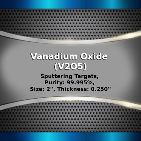
Vanadium Oxide (V2O5) Sputtering Targets, Purity: 99.9%, Size: 2”, Thickness: 0.250”

$512.00

Product 

Vanadium Oxide (V2O5) Sputtering Targets, Purity: 99.9%, Size: 2'', Thickness: 0.250''

CAS No.

1314‑62‑1

Appearance

Powder

Purity

≥99%,  ≥99.9%,  ≥95%

(Other purities are also available)

APS

N/A  (Size Can be customized), Ask for other available size ranges.

Ingredient

N/A

Molecular Weight

181.88 g/mol

Melting Point

690 °C

Boiling Point

~1750 °C

Density

~3.35 g/cm³

Product Codes

NCZ-1540K

Tungsten (W) Sputtering Targets, Purity: 99.95%, Size: 4”, Thickness: 0.250”

$511.00

Applications of Sputtering Targets;

Film deposition is accomplished using sputtering targets. A technique for sputtering thin films is called "deposition made by sputter targets," which entails eroding material from a "target" source onto a "substrate" like a silicon wafer. Etching of the target is done using semiconductor sputtering targets. When selectivity is not an issue and a high degree of etching anisotropy is required, sputter etching is the method of choice. By removing the target material through etching, sputter targets are also utilized for investigation. In secondary ion spectroscopy (SIMS), one example is when the target material is sputtered at a steady pace. Mass spectrometry is used to quantify the concentration and identity of spewed atoms as the target is sputtered.

The target material's composition may be ascertained and even very low concentrations of contaminants can be found with the aid of the sputtering target.

There is also an application area for sputtering targets in space. One type of space weathering that alters the chemical and physical characteristics of airless worlds like the Moon and asteroids is sputtering.

Nickel Oxide (NiO) Sputtering Targets, Purity: 99.9%, Size:1”, Thickness: 0.125”

$511.00

Applications of Sputtering Targets;

Film deposition is accomplished using sputtering targets. A technique for sputtering thin films is called "deposition made by sputter targets," which entails eroding material from a "target" source onto a "substrate" like a silicon wafer. Etching of the target is done using semiconductor sputtering targets. When selectivity is not an issue and a high degree of etching anisotropy is required, sputter etching is the method of choice. By removing the target material through etching, sputter targets are also utilized for investigation. In secondary ion spectroscopy (SIMS), one example is when the target material is sputtered at a steady pace. Mass spectrometry is used to quantify the concentration and identity of spewed atoms as the target is sputtered.

The target material's composition may be ascertained and even very low concentrations of contaminants can be found with the aid of the sputtering target.

There is also an application area for sputtering targets in space. One type of space weathering that alters the chemical and physical characteristics of airless worlds like the Moon and asteroids is sputtering.

Lithium Cobalt Oxide (LiCoO2) Sputtering Targets, Purity: 99.9%, Size: 2”, Thickness: 0.125”

$511.00

Applications of Sputtering Targets;

Film deposition is accomplished using sputtering targets. A technique for sputtering thin films is called "deposition made by sputter targets," which entails eroding material from a "target" source onto a "substrate" like a silicon wafer. Etching of the target is done using semiconductor sputtering targets. When selectivity is not an issue and a high degree of etching anisotropy is required, sputter etching is the method of choice. By removing the target material through etching, sputter targets are also utilized for investigation. In secondary ion spectroscopy (SIMS), one example is when the target material is sputtered at a steady pace. Mass spectrometry is used to quantify the concentration and identity of spewed atoms as the target is sputtered.

The target material's composition may be ascertained and even very low concentrations of contaminants can be found with the aid of the sputtering target.

There is also an application area for sputtering targets in space. One type of space weathering that alters the chemical and physical characteristics of airless worlds like the Moon and asteroids is sputtering.

Formula LiCoO2 represents the chemical compound lithium cobalt oxide. A crystalline solid that is dark blue or bluish-gray in color, lithium cobalt oxide is frequently utilized in the positive electrodes of lithium-ion batteries.

Ytterbium Oxide (Yb2O3) Sputtering Targets, Purity: 99.9%, Size: 2”, Thickness: 0.125”

$511.00

Applications of Sputtering Targets;

  • Sputtering targets is used for film deposition. The deposition made by sputter targets is a method of depositing thin films by sputtering that involves eroding material from a "target" source onto a "substrate" such as  a silicon wafer.
  • Semiconductor sputtering targets is used to etch the target. Sputter etching is chosen in cases where a high degree of etching anisotropy is needed and selectivity is not a concern.
  • Sputter targets is also used for analysis by etching away the target material.
One of the example occurs in secondary ion spectroscopy (SIMS), where the target sample is sputtered at a constant rate. As the target is sputtered, the concentration and identity of sputtered atoms are measured using mass spectrometry. By helping of the sputtering target, the composition of the target material can be determined and even extremely low concentrations of impurities are detected. Sputtering target has also application area in space. Sputtering is one of the forms of space weathering, a process that changes the physical and chemical properties of airless bodies, such as asteroids and the Moon.

Lanthanum Strontium Manganate (La0.9Sr0.1MnO3) Sputtering Targets, Purity: 99.9%, Size: 3”, Thickness: 0.125”

$511.00

Applications of Sputtering Targets;

  • Sputtering targets is used for film deposition. The deposition made by sputter targets is a method of depositing thin films by sputtering that involves eroding material from a "target" source onto a "substrate" such as  a silicon wafer.
  • Semiconductor sputtering targets is used to etch the target. Sputter etching is chosen in cases where a high degree of etching anisotropy is needed and selectivity is not a concern.
  • Sputter targets is also used for analysis by etching away the target material.
One of the example occurs in secondary ion spectroscopy (SIMS), where the target sample is sputtered at a constant rate. As the target is sputtered, the concentration and identity of sputtered atoms are measured using mass spectrometry. By helping of the sputtering target, the composition of the target material can be determined and even extremely low concentrations of impurities are detected. Sputtering target has also application area in space. Sputtering is one of the forms of space weathering, a process that changes the physical and chemical properties of airless bodies, such as asteroids and the Moon.

Manganese (Mn) Sputtering Targets, Purity: 99.95%, Size: 6”, Thickness: 0.250”

$510.00

Applications of Sputtering Targets;

Film deposition is accomplished using sputtering targets. A technique for sputtering thin films is called "deposition made by sputter targets," which entails eroding material from a "target" source onto a "substrate" like a silicon wafer. Etching of the target is done using semiconductor sputtering targets. When selectivity is not an issue and a high degree of etching anisotropy is required, sputter etching is the method of choice. By removing the target material through etching, sputter targets are also utilized for investigation. In secondary ion spectroscopy (SIMS), one example is when the target material is sputtered at a steady pace. Mass spectrometry is used to quantify the concentration and identity of spewed atoms as the target is sputtered.

The target material's composition may be ascertained and even very low concentrations of contaminants can be found with the aid of the sputtering target.

There is also an application area for sputtering targets in space. One type of space weathering that alters the chemical and physical characteristics of airless worlds like the Moon and asteroids is sputtering.

Carbon (C) (Pyrolytic Graphite) Sputtering Targets, Purity: 99.999%, Size: 2”, Thickness: 0.250”

$510.00

Applications of Sputtering Targets;

Film deposition is accomplished using sputtering targets. A technique for sputtering thin films is called "deposition made by sputter targets," which entails eroding material from a "target" source onto a "substrate" like a silicon wafer. Etching of the target is done using semiconductor sputtering targets. When selectivity is not an issue and a high degree of etching anisotropy is required, sputter etching is the method of choice. By removing the target material through etching, sputter targets are also utilized for investigation. In secondary ion spectroscopy (SIMS), one example is when the target material is sputtered at a steady pace. Mass spectrometry is used to quantify the concentration and identity of spewed atoms as the target is sputtered.

The target material's composition may be ascertained and even very low concentrations of contaminants can be found with the aid of the sputtering target.

There is also an application area for sputtering targets in space. One type of space weathering that alters the chemical and physical characteristics of airless worlds like the Moon and asteroids is sputtering.

Boron Nitride (BN) Sputtering Targets, Purity: 99.5%, Size: 4”, Thickness: 0.125”

$510.00

Applications of Sputtering Targets;

Film deposition is accomplished using sputtering targets. A technique for sputtering thin films is called "deposition made by sputter targets," which entails eroding material from a "target" source onto a "substrate" like a silicon wafer. Etching of the target is done using semiconductor sputtering targets. When selectivity is not an issue and a high degree of etching anisotropy is required, sputter etching is the method of choice. By removing the target material through etching, sputter targets are also utilized for investigation. In secondary ion spectroscopy (SIMS), one example is when the target material is sputtered at a steady pace. Mass spectrometry is used to quantify the concentration and identity of spewed atoms as the target is sputtered.

The target material's composition may be ascertained and even very low concentrations of contaminants can be found with the aid of the sputtering target.

There is also an application area for sputtering targets in space. One type of space weathering that alters the chemical and physical characteristics of airless worlds like the Moon and asteroids is sputtering.