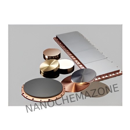
Tungsten Oxide (WO3) Sputtering Targets, Purity: 99.9%, Size: 4”, Thickness: 0.250”

$1,843.00

Applications of Sputtering Targets;

Film deposition is accomplished using sputtering targets. A technique for sputtering thin films is called "deposition made by sputter targets," which entails eroding material from a "target" source onto a "substrate" like a silicon wafer. Etching of the target is done using semiconductor sputtering targets. When selectivity is not an issue and a high degree of etching anisotropy is required, sputter etching is the method of choice. By removing the target material through etching, sputter targets are also utilized for investigation. In secondary ion spectroscopy (SIMS), one example is when the target material is sputtered at a steady pace. Mass spectrometry is used to quantify the concentration and identity of spewed atoms as the target is sputtered.

The target material's composition may be ascertained and even very low concentrations of contaminants can be found with the aid of the sputtering target.

There is also an application area for sputtering targets in space. One type of space weathering that alters the chemical and physical characteristics of airless worlds like the Moon and asteroids is sputtering.

Praseodymium Calcium Manganate (Pr0.7Ca0.3MnO3) Sputtering Targets, Purity: 99.9%, Size: 4”, Thickness: 0.125”

$1,834.00

Product 

Praseodymium Calcium Manganate (Pr0.7Ca0.3MnO3) Sputtering Targets, Purity: 99.9%, Size: 4'', Thickness: 0.125''

CAS No.

N/A

Appearance

Powder

Purity

≥99%,  ≥99.9%,  ≥95%

(Other purities are also available)

APS

1–5 μm (Size Can be customized), Ask for other available size ranges.

Ingredient

N/A

Molecular Weight

237.66 g/mol

Melting Point

N/A

Boiling Point

N/A

Density

~6.4–6.8 g/cm³

Product Codes

NCZ-1777K

Europium (Eu) Sputtering Target

Price range: $515.00 through $1,814.00
Select options This product has multiple variants. The options may be chosen on the product page

Product 

Europium (Eu) Sputtering Target

CAS No.

7440-53-1

Appearance

Powder

Purity

≥99%,  ≥99.9%,  ≥95%

(Other purities are also available)

APS

 NA (Size Can be customized), Ask for other available size ranges.

Ingredient

N/A

Molecular Weight

151.964 g/mol

Melting Point

826 °C

Boiling Point

1,529 °C

Density

~5.24 g/cm³

Product Codes

NCZ-1288K

Bismuth Telluride (Bi2Te3) Sputtering Targets, Purity: 99.999%, Size: 8”, Thickness: 0.250”

$1,810.00

Applications of Sputtering Targets;

Film deposition is accomplished using sputtering targets. A technique for sputtering thin films is called "deposition made by sputter targets," which entails eroding material from a "target" source onto a "substrate" like a silicon wafer. Etching of the target is done using semiconductor sputtering targets. When selectivity is not an issue and a high degree of etching anisotropy is required, sputter etching is the method of choice. By removing the target material through etching, sputter targets are also utilized for investigation. In secondary ion spectroscopy (SIMS), one example is when the target material is sputtered at a steady pace. Mass spectrometry is used to quantify the concentration and identity of spewed atoms as the target is sputtered.

The target material's composition may be ascertained and even very low concentrations of contaminants can be found with the aid of the sputtering target.

There is also an application area for sputtering targets in space. One type of space weathering that alters the chemical and physical characteristics of airless worlds like the Moon and asteroids is sputtering.

Bi2Te3, or bismuth telluride, is a gray powder that is a combination of bismuth and tellurium. It is a semiconductor that becomes an effective thermoelectric material for refrigeration or portable power generation when alloyed with antimony or selenium. Since Bi2Te3 is a topological insulator, its physical characteristics depend on its thickness.

Lead Zirconium Titanate/PZT (O5PbTiZr) Sputtering Targets, Purity: 99.9%, Size: 4”, Thickness: 0.125”

$1,806.00

Applications of Sputtering Targets;

Film deposition is accomplished using sputtering targets. A technique for sputtering thin films is called "deposition made by sputter targets," which entails eroding material from a "target" source onto a "substrate" like a silicon wafer. Etching of the target is done using semiconductor sputtering targets. When selectivity is not an issue and a high degree of etching anisotropy is required, sputter etching is the method of choice. By removing the target material through etching, sputter targets are also utilized for investigation. In secondary ion spectroscopy (SIMS), one example is when the target material is sputtered at a steady pace. Mass spectrometry is used to quantify the concentration and identity of spewed atoms as the target is sputtered.

The target material's composition may be ascertained and even very low concentrations of contaminants can be found with the aid of the sputtering target.

There is also an application area for sputtering targets in space. One type of space weathering that alters the chemical and physical characteristics of airless worlds like the Moon and asteroids is sputtering.

An inorganic substance is lead zirconium titanate. This ceramic perovskite material has a strong piezoelectric effect, which means that when an electric field is applied, the compound changes shape. Lead zirconium titanate is employed in a number of practical applications such as ultrasonic transducers and piezoelectric resonators.

Lithium Phosphate (Li3PO4) Sputtering Targets, Purity: 99.95%, Size: 6”, Thickness: 0.125”

$1,803.00

Product 

Lithium Phosphate (Li3PO4) Sputtering Targets, Purity: 99.95%, Size: 6'', Thickness: 0.125''

CAS No.

10377-52-3

Appearance

Powder

Purity

≥99%,  ≥99.9%,  ≥95%

(Other purities are also available)

APS

 N/A (Size Can be customized), Ask for other available size ranges.

Ingredient

N/A

Molecular Weight

 115.79 g/mol

Melting Point

 ~837 °C

Boiling Point

N/A

Density

 ~2.53 g/cm³

Product Codes

NCZ-2025K

Barium Strontium Titanate (BaO4SrTi) Sputtering Targets, elastomer, Purity: 99.99%, Size: 3”, Thickness: 0.250”

$1,800.00

Product 

Barium Strontium Titanate (BaO4SrTi) Sputtering Targets, elastomer, Purity: 99.99%, Size: 3'', Thickness: 0.250''

CAS No.

 12060-08-1

Appearance

Powder

Purity

≥99%,  ≥99.9%,  ≥95%

(Other purities are also available)

APS

~1–5 µm (Size Can be customized), Ask for other available size ranges.

Ingredient

N/A

Molecular Weight

~233–300 g/mol (composition dependent)

Melting Point

 ~1625 °C (approximate)

Boiling Point

N/A

Density

~5.5–6.0 g/cm³ (depending on Ba:Sr ratio)

Product Codes

NCZ-2473K

Tungsten Oxide (WO3) Sputtering Targets, indium, Purity: 99.9%, Size: 3”, Thickness: 0.125”

$1,800.00

Product 

Tungsten Oxide (WO3) Sputtering Targets, indium, Purity: 99.9%, Size: 3'', Thickness: 0.125''

CAS No.

1314-35-8

Appearance

Powder

Purity

≥99%,  ≥99.9%,  ≥95%

(Other purities are also available)

APS

N/A  (Size Can be customized), Ask for other available size ranges.

Ingredient

N/A

Molecular Weight

231.84 g/mol

Melting Point

1,473 °C

Boiling Point

1,700–1,850 °C

Density

7.16 g/cm³

Product Codes

NCZ-1565K

Titanium Dioxide (TiO2) Sputtering Targets, Purity: 99.99%, Size: 4”, Thickness: 0.125”, Beige to White

$1,800.00

Product 

Titanium Dioxide (TiO2) Sputtering Targets, Purity: 99.99%, Size: 4'', Thickness: 0.125'', Beige to White

CAS No.

13463‑67‑7

Appearance

Powder

Purity

≥99%,  ≥99.9%,  ≥95%

(Other purities are also available)

APS

TiO₂ (black granules) (Size Can be customized), Ask for other available size ranges.

Ingredient

N/A

Molecular Weight

79.94 g/mol

Melting Point

~1,843 °C

Boiling Point

~2,972 °C

Density

~4.23 g/cm³

Product Codes

NCZ-1432K

Lead Zirconium Titanate/PZT (O5PbTiZr) Sputtering Targets, Purity: 99.9%, Size: 6”, Thickness: 0.250”

$1,800.00

Applications of Sputtering Targets;

Film deposition is accomplished using sputtering targets. A technique for sputtering thin films is called "deposition made by sputter targets," which entails eroding material from a "target" source onto a "substrate" like a silicon wafer. Etching of the target is done using semiconductor sputtering targets. When selectivity is not an issue and a high degree of etching anisotropy is required, sputter etching is the method of choice. By removing the target material through etching, sputter targets are also utilized for investigation. In secondary ion spectroscopy (SIMS), one example is when the target material is sputtered at a steady pace. Mass spectrometry is used to quantify the concentration and identity of spewed atoms as the target is sputtered.

The target material's composition may be ascertained and even very low concentrations of contaminants can be found with the aid of the sputtering target.

There is also an application area for sputtering targets in space. One type of space weathering that alters the chemical and physical characteristics of airless worlds like the Moon and asteroids is sputtering.

An inorganic substance is lead zirconium titanate. This ceramic perovskite material has a strong piezoelectric effect, which means that when an electric field is applied, the compound changes shape. Lead zirconium titanate is employed in a number of practical applications such as ultrasonic transducers and piezoelectric resonators.

Lithium Phosphate (Li3PO4) Sputtering Targets, Purity: 99.95%, Size: 7”, Thickness: 0.250”

$1,797.00

Applications of Sputtering Targets;

Film deposition is accomplished using sputtering targets. A technique for sputtering thin films is called "deposition made by sputter targets," which entails eroding material from a "target" source onto a "substrate" like a silicon wafer. Etching of the target is done using semiconductor sputtering targets. When selectivity is not an issue and a high degree of etching anisotropy is required, sputter etching is the method of choice. By removing the target material through etching, sputter targets are also utilized for investigation. In secondary ion spectroscopy (SIMS), one example is when the target material is sputtered at a steady pace. Mass spectrometry is used to quantify the concentration and identity of spewed atoms as the target is sputtered.

By helping of the sputtering target, the composition of the target material may be evaluated and even extremely tiny amounts of contaminants are recognized.

There is also an application area for sputtering targets in space. One type of space weathering that alters the chemical and physical characteristics of airless worlds like the Moon and asteroids is sputtering.

Lead Telluride (PbTe) Sputtering Target

Price range: $566.00 through $1,794.00
Select options This product has multiple variants. The options may be chosen on the product page

Product 

Lead Telluride (PbTe) Sputtering Target

CAS No.

1314-91-6

Appearance

Powder

Purity

≥99%,  ≥99.9%,  ≥95%

(Other purities are also available)

APS

 NA (Size Can be customized), Ask for other available size ranges.

Ingredient

N/A

Molecular Weight

 334.8 g/mol

Melting Point

~924 °C

Boiling Point

~1,476 °C

Density

~8.16 g/cm³

Product Codes

NCZ-1345K

Barium Strontium Titanate (BaO4SrTi) Sputtering Targets, elastomer, Purity: 99.99%, Size: 4”, Thickness: 0.250”

$1,789.00

Product 

Barium Strontium Titanate (BaO4SrTi) Sputtering Targets, elastomer, Purity: 99.99%, Size: 4'', Thickness: 0.250''

CAS No.

 12060-08-1

Appearance

Powder

Purity

≥99%,  ≥99.9%,  ≥95%

(Other purities are also available)

APS

~1–5 µm (Size Can be customized), Ask for other available size ranges.

Ingredient

N/A

Molecular Weight

~233–300 g/mol (composition dependent)

Melting Point

 ~1625 °C (approximate)

Boiling Point

N/A

Density

~5.5–6.0 g/cm³ (depending on Ba:Sr ratio)

Product Codes

NCZ-2471K

Barium Fluoride (BaF2) Sputtering Targets, Purity: 99.99%, Size: 5”, Thickness: 0.125”

$1,777.00

Product 

Barium Fluoride (BaF2) Sputtering Targets, Purity: 99.99%, Size: 5'', Thickness: 0.125''

CAS No.

 7787-32-8

Appearance

Powder

Purity

≥99%,  ≥99.9%,  ≥95%

(Other purities are also available)

APS

< 5 µm (Size Can be customized), Ask for other available size ranges.

Ingredient

N/A

Molecular Weight

175.32 g/mol

Melting Point

 1,368 °C

Boiling Point

2,260 °C

Density

 4.89 g/cm³

Product Codes

NCZ-2481K

Barium Fluoride (BaF2) Sputtering Targets, Purity: 99.99%, Size: 5”, Thickness: 0.250”

$1,777.00

Product 

Barium Fluoride (BaF2) Sputtering Targets, Purity: 99.99%, Size: 5'', Thickness: 0.250''

CAS No.

 7787-32-8

Appearance

Powder

Purity

≥99%,  ≥99.9%,  ≥95%

(Other purities are also available)

APS

< 5 µm (Size Can be customized), Ask for other available size ranges.

Ingredient

N/A

Molecular Weight

175.32 g/mol

Melting Point

 1,368 °C

Boiling Point

2,260 °C

Density

 4.89 g/cm³

Product Codes

NCZ-2480K

Titanium Dioxide (TiO2) Sputtering Targets, Purity: 99.99%, Size: 4”, Thickness: 0.250”, Beige to White

$1,751.00

Applications of Sputtering Targets;

Film deposition is accomplished using sputtering targets. A technique for sputtering thin films is called "deposition made by sputter targets," which entails eroding material from a "target" source onto a "substrate" like a silicon wafer. Etching of the target is done using semiconductor sputtering targets. When selectivity is not an issue and a high degree of etching anisotropy is required, sputter etching is the method of choice. By removing the target material through etching, sputter targets are also utilized for investigation. In secondary ion spectroscopy (SIMS), one example is when the target material is sputtered at a steady pace. Mass spectrometry is used to quantify the concentration and identity of spewed atoms as the target is sputtered.

The target material's composition may be ascertained and even very low concentrations of contaminants can be found with the aid of the sputtering target.

There is also an application area for sputtering targets in space. One type of space weathering that alters the chemical and physical characteristics of airless worlds like the Moon and asteroids is sputtering.

Lithium Phosphate (Li3PO4) Sputtering Targets, elastomer, Purity: 99.95%, Size: 4”, Thickness: 0.125”

$1,750.00

Product 

Lithium Phosphate (Li3PO4) Sputtering Targets, elastomer, Purity: 99.95%, Size: 4'', Thickness: 0.125''

CAS No.

10377-52-3

Appearance

Powder

Purity

≥99%,  ≥99.9%,  ≥95%

(Other purities are also available)

APS

 N/A (Size Can be customized), Ask for other available size ranges.

Ingredient

N/A

Molecular Weight

 115.79 g/mol

Melting Point

 ~837 °C

Boiling Point

N/A

Density

 ~2.53 g/cm³

Product Codes

NCZ-2016K

Bismuth Telluride (Bi2Te3) Sputtering Targets, Purity: 99.999%, Size: 6”, Thickness: 0.250”

$1,750.00

Applications of Sputtering Targets;

Film deposition is accomplished using sputtering targets. A technique for sputtering thin films is called "deposition made by sputter targets," which entails eroding material from a "target" source onto a "substrate" like a silicon wafer. Etching of the target is done using semiconductor sputtering targets. When selectivity is not an issue and a high degree of etching anisotropy is required, sputter etching is the method of choice. By removing the target material through etching, sputter targets are also utilized for investigation. In secondary ion spectroscopy (SIMS), one example is when the target material is sputtered at a steady pace. Mass spectrometry is used to quantify the concentration and identity of spewed atoms as the target is sputtered.

The target material's composition may be ascertained and even very low concentrations of contaminants can be found with the aid of the sputtering target.

There is also an application area for sputtering targets in space. One type of space weathering that alters the chemical and physical characteristics of airless worlds like the Moon and asteroids is sputtering.

Bi2Te3, or bismuth telluride, is a gray powder that is a combination of bismuth and tellurium. It is a semiconductor that becomes an effective thermoelectric material for refrigeration or portable power generation when alloyed with antimony or selenium. Since Bi2Te3 is a topological insulator, its physical characteristics depend on its thickness.

Lead Zirconium Titanate/PZT (O5PbTiZr) Sputtering Targets, Purity: 99.9%, Size: 4”, Thickness: 0.250”

$1,732.00

Product 

Lead Zirconium Titanate/PZT (O5PbTiZr) Sputtering Targets, Purity: 99.9%, Size: 4'', Thickness: 0.250''

CAS No.

12626-81-2

Appearance

Powder

Purity

≥99%,  ≥99.9%,  ≥95%

(Other purities are also available)

APS

 N/A (Size Can be customized), Ask for other available size ranges.

Ingredient

N/A

Molecular Weight

~303.1 g/mol

Melting Point

 ~1,250°C – 1,350°C

Boiling Point

N/A

Density

 ~7.75–8.0 g/cm³

Product Codes

NCZ-2063K

Tungsten Oxide (WO3) Sputtering Targets, Purity: 99.9%, Size: 4”, Thickness: 0.125”

$1,717.00

Applications of Sputtering Targets;

Film deposition is done using puttering targets. A technique for sputtering thin films is called "deposition made by sputter targets," which entails eroding material from a "target" source onto a "substrate" like a silicon wafer. Etching of the target is done using semiconductor sputtering targets. When selectivity is not an issue and a high degree of etching anisotropy is required, sputter etching is the method of choice. By removing the target material through etching, sputter targets are also utilized for investigation. In secondary ion spectroscopy (SIMS), one example is when the target material is sputtered at a steady pace. Mass spectrometry is used to quantify the concentration and identity of spewed atoms as the target is sputtered.

The target material's composition may be ascertained and even very low concentrations of contaminants can be found with the aid of the sputtering target.

There is also an application area for sputtering targets in space. One type of space weathering that alters the chemical and physical characteristics of airless worlds like the Moon and asteroids is sputtering.

Lithium Phosphate (Li3PO4) Sputtering Targets, Purity: 99.95%, Size: 7”, Thickness: 0.125”

$1,716.00

Applications of Sputtering Targets;

Film deposition is accomplished using sputtering targets. A technique for sputtering thin films is called "deposition made by sputter targets," which entails eroding material from a "target" source onto a "substrate" like a silicon wafer. Etching of the target is done using semiconductor sputtering targets. When selectivity is not an issue and a high degree of etching anisotropy is required, sputter etching is the method of choice. By removing the target material through etching, sputter targets are also utilized for investigation. In secondary ion spectroscopy (SIMS), one example is when the target material is sputtered at a steady pace. Mass spectrometry is used to quantify the concentration and identity of spewed atoms as the target is sputtered.

By helping of the sputtering target, the composition of the target material may be evaluated and even extremely tiny amounts of contaminants are recognized.

There is also an application area for sputtering targets in space. One type of space weathering that alters the chemical and physical characteristics of airless worlds like the Moon and asteroids is sputtering.

Boron Nitride (BN) Sputtering Targets, Purity: 99.5%, Size: 8”, Thickness: 0.250”

$1,709.00

Product 

Boron Nitride (BN) Sputtering Targets, Purity: 99.5%, Size: 8'', Thickness: 0.250''

CAS No.

12058-85-6

Appearance

Powder

Purity

≥99%,  ≥99.9%,  ≥95%

(Other purities are also available)

APS

 N/A (Size Can be customized), Ask for other available size ranges.

Ingredient

N/A

Molecular Weight

157.93 g/mol

Melting Point

~1400 °C (decomposes)

Boiling Point

N/A

Density

~4.3 - 4.7 g/cm³ (varies with form)

Product Codes

NCZ-2364K

Cerium Oxide (CeO2) Sputtering Targets, Purity: 99.99%, Size: 8”, Thickness: 0.125”

$1,683.00

Product 

Cerium Oxide (CeO2) Sputtering Targets, Purity: 99.99%, Size: 8'', Thickness: 0.125''

CAS No.

 1306-38-3

Appearance

Powder

Purity

≥99%,  ≥99.9%,  ≥95%

(Other purities are also available)

APS

 N/A (Size Can be customized), Ask for other available size ranges.

Ingredient

N/A

Molecular Weight

 172.11 g/mol

Melting Point

2,400–2,600 °C

Boiling Point

Sublimes above 3,000 °C

Density

 7.13 g/cm³

Product Codes

NCZ-2319K

Lead Zirconium Titanate/PZT (O5PbTiZr) Sputtering Targets, Purity: 99.9%, Size: 7”, Thickness: 0.250”

$1,683.00

Product 

Lead Zirconium Titanate/PZT (O5PbTiZr) Sputtering Targets, Purity: 99.9%, Size: 8'', Thickness: 0.125''

CAS No.

12626-81-2

Appearance

Powder

Purity

≥99%,  ≥99.9%,  ≥95%

(Other purities are also available)

APS

 N/A (Size Can be customized), Ask for other available size ranges.

Ingredient

N/A

Molecular Weight

~303.1 g/mol

Melting Point

 ≈ 1,250–1,350 °C (ceramic decomposes)

Boiling Point

N/A

Density

 ~7.75–8.0 g/cm³

Product Codes

NCZ-2057K

Praseodymium Calcium Manganate (Pr0.7Ca0.3MnO3) Sputtering Targets, Purity: 99.9%, Size: 4”, Thickness: 0.250”

$1,675.00

Applications of Sputtering Targets;

Film deposition is accomplished using sputtering targets. A technique for sputtering thin films is called "deposition made by sputter targets," which entails eroding material from a "target" source onto a "substrate" like a silicon wafer. Etching of the target is done using semiconductor sputtering targets. When selectivity is not an issue and a high degree of etching anisotropy is required, sputter etching is the method of choice. By removing the target material through etching, sputter targets are also utilized for investigation. In secondary ion spectroscopy (SIMS), one example is when the target material is sputtered at a steady pace. Mass spectrometry is used to quantify the concentration and identity of spewed atoms as the target is sputtered.

The target material's composition may be ascertained and even very low concentrations of contaminants can be found with the aid of the sputtering target.

There is also an application area for sputtering targets in space. One type of space weathering that alters the chemical and physical characteristics of airless worlds like the Moon and asteroids is sputtering.

Praseodymium Calcium Manganate (Pr0.7Ca0.3MnO3) Sputtering Targets, Purity: 99.9%, Size: 4”, Thickness: 0.250”

$1,675.00

Applications of Sputtering Targets;

  • Sputtering targets is used for film deposition. The deposition made by sputter targets is a method of depositing thin films by sputtering that involves eroding material from a "target" source onto a "substrate" such as  a silicon wafer.
  • Semiconductor sputtering targets is used to etch the target. Sputter etching is chosen in cases where a high degree of etching anisotropy is needed and selectivity is not a concern.
  • Sputter targets is also used for analysis by etching away the target material.
One of the example occurs in secondary ion spectroscopy (SIMS), where the target sample is sputtered at a constant rate. As the target is sputtered, the concentration and identity of sputtered atoms are measured using mass spectrometry. By helping of the sputtering target, the composition of the target material can be determined and even extremely low concentrations of impurities are detected. Sputtering target has also application area in space. Sputtering is one of the forms of space weathering, a process that changes the physical and chemical properties of airless bodies, such as asteroids and the Moon.

Titanium Dioxide (TiO2) Sputtering Targets, Purity: 99.99%, Size: 3”, Thickness: 0.125”, Beige to White

$1,666.00

Product 

Titanium Dioxide (TiO2) Sputtering Targets, Purity: 99.99%, Size: 3'', Thickness: 0.125'', Beige to White

CAS No.

13463‑67‑7

Appearance

Powder

Purity

≥99%,  ≥99.9%,  ≥95%

(Other purities are also available)

APS

TiO₂ (black granules) (Size Can be customized), Ask for other available size ranges.

Ingredient

N/A

Molecular Weight

79.94 g/mol

Melting Point

~1,843 °C

Boiling Point

~2,972 °C

Density

~4.23 g/cm³

Product Codes

NCZ-1418K

Bismuth Telluride (Bi2Te3) Sputtering Targets, Purity: 99.999%, Size: 4”, Thickness: 0.125”

$1,665.00

Applications of Sputtering Targets;.

Film deposition is accomplished using sputtering targets. A technique for sputtering thin films is called "deposition made by sputter targets," which entails eroding material from a "target" source onto a "substrate" like a silicon wafer. Etching of the target is done using semiconductor sputtering targets. When selectivity is not an issue and a high degree of etching anisotropy is required, sputter etching is the method of choice. By removing the target material through etching, sputter targets are also utilized for investigation. In secondary ion spectroscopy (SIMS), one example is when the target material is sputtered at a steady pace. Mass spectrometry is used to quantify the concentration and identity of spewed atoms as the target is sputtered.

The target material's composition may be ascertained and even very low concentrations of contaminants can be found with the aid of the sputtering target.

There is also an application area for sputtering targets in space. One type of space weathering that alters the chemical and physical characteristics of airless worlds like the Moon and asteroids is sputtering.

Bi2Te3, or bismuth telluride, is a gray powder that is a combination of bismuth and tellurium. It is a semiconductor that becomes an effective thermoelectric material for refrigeration or portable power generation when alloyed with antimony or selenium. Since Bi2Te3 is a topological insulator, its physical characteristics depend on its thickness.

Bismuth Telluride (Bi2Te3) Sputtering Targets, Purity: 99.999%, Size: 4”, Thickness: 0.250”

$1,665.00

Applications of Sputtering Targets;

Film deposition is accomplished using sputtering targets. A technique for sputtering thin films is called "deposition made by sputter targets," which entails eroding material from a "target" source onto a "substrate" like a silicon wafer. Etching of the target is done using semiconductor sputtering targets. When selectivity is not an issue and a high degree of etching anisotropy is required, sputter etching is the method of choice. By removing the target material through etching, sputter targets are also utilized for investigation. In secondary ion spectroscopy (SIMS), one example is when the target material is sputtered at a steady pace. Mass spectrometry is used to quantify the concentration and identity of spewed atoms as the target is sputtered.

The target material's composition may be ascertained and even very low concentrations of contaminants can be found with the aid of the sputtering target.

There is also an application area for sputtering targets in space. One type of space weathering that alters the chemical and physical characteristics of airless worlds like the Moon and asteroids is sputtering.

Bi2Te3, or bismuth telluride, is a gray powder that is a combination of bismuth and tellurium. It is a semiconductor that becomes an effective thermoelectric material for refrigeration or portable power generation when alloyed with antimony or selenium. Since Bi2Te3 is a topological insulator, its physical characteristics depend on its thickness.

Lead Zirconium Titanate/PZT (O5PbTiZr) Sputtering Targets, Purity: 99.9%, Size: 5”, Thickness: 0.250”

$1,663.00

Product 

Lead Zirconium Titanate/PZT (O5PbTiZr) Sputtering Targets, Purity: 99.9%, Size: 5'', Thickness: 0.250''

CAS No.

12626-81-2

Appearance

Powder

Purity

≥99%,  ≥99.9%,  ≥95%

(Other purities are also available)

APS

 N/A (Size Can be customized), Ask for other available size ranges.

Ingredient

N/A

Molecular Weight

~303.1 g/mol

Melting Point

 ~1,250°C – 1,350°C

Boiling Point

N/A

Density

 ~7.75–8.0 g/cm³

Product Codes

NCZ-2061K

Lead Zirconium Titanate/PZT (O5PbTiZr) Sputtering Targets, Purity: 99.9%, Size: 6”, Thickness: 0.125”

$1,663.00

Product 

Lead Zirconium Titanate/PZT (O5PbTiZr) Sputtering Targets, Purity: 99.9%, Size: 6'', Thickness: 0.125''

CAS No.

12626-81-2

Appearance

Powder

Purity

≥99%,  ≥99.9%,  ≥95%

(Other purities are also available)

APS

 N/A (Size Can be customized), Ask for other available size ranges.

Ingredient

N/A

Molecular Weight

~303.1 g/mol

Melting Point

 ~1,250°C – 1,350°C

Boiling Point

N/A

Density

 ~7.75–8.0 g/cm³

Product Codes

NCZ-2060K

Magnesium Oxide (MgO) Sputtering Targets, Purity: 99.95%, Size: 4”, Thickness: 0.250”

$1,657.00

Product 

Magnesium Oxide (MgO) Sputtering Targets, Purity: 99.95%, Size: 4'', Thickness: 0.250''

CAS No.

1309-48-4

Appearance

Powder

Purity

≥99%,  ≥99.9%,  ≥95%

(Other purities are also available)

APS

 N/A (Size Can be customized), Ask for other available size ranges.

Ingredient

N/A

Molecular Weight

40.30 g/mol

Melting Point

 ~2852 °C

Boiling Point

~3600 °C

Density

 ~3.58 g/cm³

Product Codes

NCZ-1969K

Lithium Phosphate (Li3PO4) Sputtering Targets, Purity: 99.95%, Size: 6”, Thickness: 0.250”

$1,653.00

Applications of Sputtering Targets;

Film deposition is accomplished using sputtering targets. A technique for sputtering thin films is called "deposition made by sputter targets," which entails eroding material from a "target" source onto a "substrate" like a silicon wafer. Etching of the target is done using semiconductor sputtering targets. When selectivity is not an issue and a high degree of etching anisotropy is required, sputter etching is the method of choice. By removing the target material through etching, sputter targets are also utilized for investigation. In secondary ion spectroscopy (SIMS), one example is when the target material is sputtered at a steady pace. Mass spectrometry is used to quantify the concentration and identity of spewed atoms as the target is sputtered.

By helping of the sputtering target, the composition of the target material may be evaluated and even extremely tiny amounts of contaminants are recognized.

There is also an application area for sputtering targets in space. One type of space weathering that alters the chemical and physical characteristics of airless worlds like the Moon and asteroids is sputtering.

Lead Zirconium Titanate/PZT (O5PbTiZr) Sputtering Targets, Purity: 99.9%, Size: 8”, Thickness: 0.125”

$1,642.00

Product 

Lead Zirconium Titanate/PZT (O5PbTiZr) Sputtering Targets, Purity: 99.9%, Size: 8'', Thickness: 0.125''

CAS No.

12626-81-2

Appearance

Powder

Purity

≥99%,  ≥99.9%,  ≥95%

(Other purities are also available)

APS

 N/A (Size Can be customized), Ask for other available size ranges.

Ingredient

N/A

Molecular Weight

~303.07 g/mol

Melting Point

 >1,250 °C (PZT decomposes or sinters, doesn’t boil)

Boiling Point

N/A

Density

 ~7.6–8.0 g/cm³(depends on stoichiometry and porosity)

Product Codes

NCZ-2056K

Cerium Oxide (CeO2) Sputtering Targets, indium, Purity: 99.99%, Size: 4”, Thickness: 0.125”

$1,638.00

Applications of Sputtering Targets;

Film deposition is accomplished using sputtering targets. A technique for sputtering thin films is called "deposition made by sputter targets," which entails eroding material from a "target" source onto a "substrate" like a silicon wafer. Etching of the target is done using semiconductor sputtering targets. When selectivity is not an issue and a high degree of etching anisotropy is required, sputter etching is the method of choice. By removing the target material through etching, sputter targets are also utilized for investigation. In secondary ion spectroscopy (SIMS), one example is when the target material is sputtered at a steady pace. Mass spectrometry is used to quantify the concentration and identity of spewed atoms as the target is sputtered.

The target material's composition may be ascertained and even very low concentrations of contaminants can be found with the aid of the sputtering target.

There is also an application area for sputtering targets in space. One type of space weathering that alters the chemical and physical characteristics of airless worlds like the Moon and asteroids is sputtering.

The most prevalent rare-earth element in the crust of the earth is cerium, a metal that belongs to the lanthanide series. Cerium oxide's high refractive index and dielectric constant make it suitable for a wide range of optical and electrical applications. Additionally, cerium oxide can be used for corrosion protection coatings rather than coatings based on chromate.

Barium Strontium Titanate (BaO4SrTi) Sputtering Targets, elastomer, Purity: 99.99%, Size: 6”, Thickness: 0.125”

$1,635.00

Applications of Sputtering Targets;

Film deposition is accomplished using sputtering targets. A technique for sputtering thin films is called "deposition made by sputter targets," which entails eroding material from a "target" source onto a "substrate" like a silicon wafer. Etching of the target is done using semiconductor sputtering targets. When selectivity is not an issue and a high degree of etching anisotropy is required, sputter etching is the method of choice. By removing the target material through etching, sputter targets are also utilized for investigation. In secondary ion spectroscopy (SIMS), one example is when the target material is sputtered at a steady pace. Mass spectrometry is used to quantify the concentration and identity of spewed atoms as the target is sputtered. With the sputtering target's assistance, the

It is possible to identify the target material and even detect incredibly tiny impurity amounts.

There is also an application area for sputtering targets in space. One type of space weathering that alters the chemical and physical characteristics of airless worlds like the Moon and asteroids is sputtering.

A solid mixture of barium titanate (BaTiO3) and strontium titanate (SrTiO3) is called barium strontium titanate (BST). Sputtering techniques yield thin coatings of barium strontium titanate (BST), which confers exceptional dielectric characteristics to materials. Due to their numerous uses in tunable microwave devices like delay lines, barium strontium titanate (BST) based ferroelectric thin film devices have become more and more well-known over the past ten years.

Barium Strontium Titanate (BaO4SrTi) Sputtering Targets, elastomer, Purity: 99.99%, Size: 6”, Thickness: 0.250”

$1,635.00

Applications of Sputtering Targets;

Film deposition is accomplished using sputtering targets. A technique for sputtering thin films is called "deposition made by sputter targets," which entails eroding material from a "target" source onto a "substrate" like a silicon wafer. Etching of the target is done using semiconductor sputtering targets. When selectivity is not an issue and a high degree of etching anisotropy is required, sputter etching is the method of choice. By removing the target material through etching, sputter targets are also utilized for investigation. In secondary ion spectroscopy (SIMS), one example is when the target material is sputtered at a steady pace. When the target shatters,

Mass spectrometry measures the concentration and identity of sputtered atoms. The target material's composition may be ascertained and even very low concentrations of contaminants can be found with the aid of the sputtering target.

There is also an application area for sputtering targets in space. One type of space weathering that alters the chemical and physical characteristics of airless worlds like the Moon and asteroids is sputtering.

A solid mixture of barium titanate (BaTiO3) and strontium titanate (SrTiO3) is called barium strontium titanate (BST). Sputtering techniques yield thin coatings of barium strontium titanate (BST), which confers exceptional dielectric characteristics to materials. Due to this, BST-based barium strontium titanate

The past ten years have seen a rise in the popularity of ferroelectric thin film devices because of its numerous uses in tunable microwave devices, including phase shifters, delay lines, resonators, and varactors.

Thin films of barium strontium titanate show great promise because of their low dielectric loss, high dielectric constant, and tunability. There have been reports on the dielectric-tunable properties of barium strontium titanate films produced by various deposition processes. These properties investigate the impacts of several parameters, including grain size, Ba/Sr ratio, oxygen vacancies, and film thickness. To get more tunability and less loss, researchers have also looked at doping concentrations, high temperature annealing, and multilayer architectures.

Barium Titanate (BaTiO3) Sputtering Targets, Purity: 99.99%, Size: 6”, Thickness: 0.250”

$1,635.00

Applications of Sputtering Targets;

Film deposition is accomplished using sputtering targets. A technique for sputtering thin films is called "deposition made by sputter targets," which entails eroding material from a "target" source onto a "substrate" like a silicon wafer. Etching of the target is done using semiconductor sputtering targets. When selectivity is not an issue and a high degree of etching anisotropy is required, sputter etching is the method of choice. By removing the target material through etching, sputter targets are also utilized for investigation. In secondary ion spectroscopy (SIMS), one example is when the target material is sputtered at a steady pace. When the target shatters,

Mass spectrometry measures the concentration and identity of sputtered atoms. The target material's composition may be ascertained and even very low concentrations of contaminants can be found with the aid of the sputtering target.

There is also an application area for sputtering targets in space. One type of space weathering that alters the chemical and physical characteristics of airless worlds like the Moon and asteroids is sputtering.

Formulated as BaTiO3, barium titanate is an inorganic substance. When formed as big crystals, barium titanate is clear and has a white powdery appearance. It is a ferroelectric ceramic material with piezoelectric and photorefractive characteristics. Titanate of barium sputtering Agents have various applications. For instance, barium titanate films, which are produced by sputtering targets, can be employed in particular electronic ceramics. Barium titanate can be utilized in the building of electrical devices such as sensors, capacitors, and detectors.

Lead Zirconium Titanate/PZT (O5PbTiZr) Sputtering Targets, Purity: 99.9%, Size: 8”, Thickness: 0.250”

$1,629.00

Applications of Sputtering Targets;

Film deposition is accomplished using sputtering targets. A technique for sputtering thin films is called "deposition made by sputter targets," which entails eroding material from a "target" source onto a "substrate" like a silicon wafer. Etching of the target is done using semiconductor sputtering targets. When selectivity is not an issue and a high degree of etching anisotropy is required, sputter etching is the method of choice. By removing the target material through etching, sputter targets are also utilized for investigation. In secondary ion spectroscopy (SIMS), one example is when the target material is sputtered at a steady pace. Mass spectrometry is used to quantify the concentration and identity of spewed atoms as the target is sputtered.

The target material's composition may be ascertained and even very low concentrations of contaminants can be found with the aid of the sputtering target.

There is also an application area for sputtering targets in space. One type of space weathering that alters the chemical and physical characteristics of airless worlds like the Moon and asteroids is sputtering.

An inorganic substance is lead zirconium titanate. This ceramic perovskite material has a strong piezoelectric effect, which means that when an electric field is applied, the compound changes shape. Lead zirconium titanate is employed in a number of practical applications such as ultrasonic transducers and piezoelectric resonators.

Lutetium Oxide (Lu2O3) Sputtering Target, CAS 12032-20-1

Price range: $684.00 through $1,623.00
Select options This product has multiple variants. The options may be chosen on the product page

Product 

Lutetium Oxide (Lu2O3) Sputtering Target, CAS 12032-20-1

CAS No.

12032‑20‑1

Appearance

Powder

Purity

≥99%,  ≥99.9%,  ≥95%

(Other purities are also available)

APS

 NA (Size Can be customized), Ask for other available size ranges.

Ingredient

N/A

Molecular Weight

397.93–397.94 g/mol

Melting Point

~2,490 °C

Boiling Point

~3,980 °C

Density

~9.42 g/cm³

Product Codes

NCZ-1374K

Titanium Dioxide (TiO2) Sputtering Targets, Purity: 99.99%, Size: 6”, Thickness: 0.250”, Beige to White

$1,620.00

Applications of Sputtering Targets;

Film deposition is accomplished using sputtering targets. A technique for sputtering thin films is called "deposition made by sputter targets," which entails eroding material from a "target" source onto a "substrate" like a silicon wafer. Etching of the target is done using semiconductor sputtering targets. When selectivity is not an issue and a high degree of etching anisotropy is required, sputter etching is the method of choice. By removing the target material through etching, sputter targets are also utilized for investigation. In secondary ion spectroscopy (SIMS), one example is when the target material is sputtered at a steady pace. Mass spectrometry is used to quantify the concentration and identity of spewed atoms as the target is sputtered.

The target material's composition may be ascertained and even very low concentrations of contaminants can be found with the aid of the sputtering target.

There is also an application area for sputtering targets in space. One type of space weathering that alters the chemical and physical characteristics of airless worlds like the Moon and asteroids is sputtering.

Lead Zirconium Titanate/PZT (O5PbTiZr) Sputtering Targets, Purity: 99.9%, Size: 7”, Thickness: 0.125”

$1,620.00

Applications of Sputtering Targets;

Film deposition is accomplished using sputtering targets. A technique for sputtering thin films is called "deposition made by sputter targets," which entails eroding material from a "target" source onto a "substrate" like a silicon wafer. Etching of the target is done using semiconductor sputtering targets. When selectivity is not an issue and a high degree of etching anisotropy is required, sputter etching is the method of choice. By removing the target material through etching, sputter targets are also utilized for investigation. In secondary ion spectroscopy (SIMS), one example is when the target material is sputtered at a steady pace. Mass spectrometry is used to quantify the concentration and identity of spewed atoms as the target is sputtered.

The target material's composition may be ascertained and even very low concentrations of contaminants can be found with the aid of the sputtering target.

There is also an application area for sputtering targets in space. One type of space weathering that alters the chemical and physical characteristics of airless worlds like the Moon and asteroids is sputtering.

An inorganic substance is lead zirconium titanate. This ceramic perovskite material has a strong piezoelectric effect, which means that when an electric field is applied, the compound changes shape. Lead zirconium titanate is employed in a number of practical applications such as ultrasonic transducers and piezoelectric resonators.

Cerium Oxide (CeO2) Sputtering Targets, Purity: 99.99%, Size: 8”, Thickness: 0.250”

$1,609.00

Product 

Cerium Oxide (CeO2) Sputtering Targets, Purity: 99.99%, Size: 8'', Thickness: 0.250''

CAS No.

 1306-38-3

Appearance

Powder

Purity

≥99%,  ≥99.9%,  ≥95%

(Other purities are also available)

APS

 N/A (Size Can be customized), Ask for other available size ranges.

Ingredient

N/A

Molecular Weight

 172.11 g/mol

Melting Point

2,400–2,600 °C

Boiling Point

Sublimes above 3,000 °C

Density

 7.13 g/cm³

Product Codes

NCZ-2320K

Titanium Dioxide (TiO2) Sputtering Targets, Purity: 99.99%, Size: 8”, Thickness: 0.250”, Beige to White

$1,608.00

Applications of Sputtering Targets;

Film deposition is accomplished using sputtering targets. A technique for sputtering thin films is called "deposition made by sputter targets," which entails eroding material from a "target" source onto a "substrate" like a silicon wafer. Etching of the target is done using semiconductor sputtering targets. When selectivity is not an issue and a high degree of etching anisotropy is required, sputter etching is the method of choice. By removing the target material through etching, sputter targets are also utilized for investigation. In secondary ion spectroscopy (SIMS), one example is when the target material is sputtered at a steady pace. Mass spectrometry is used to quantify the concentration and identity of spewed atoms as the target is sputtered.

The target material's composition may be ascertained and even very low concentrations of contaminants can be found with the aid of the sputtering target.

There is also an application area for sputtering targets in space. One type of space weathering that alters the chemical and physical characteristics of airless worlds like the Moon and asteroids is sputtering.

Titanium Nitride (TiN) Sputtering Targets, indium, Purity: 99.5%, Size: 4”, Thickness: 0.125”

$1,606.00

Product 

Titanium Nitride (TiN) Sputtering Targets, indium, Purity: 99.5%, Size: 4'', Thickness: 0.125''

CAS No.

25583-20-4

Appearance

Powder

Purity

≥99%,  ≥99.9%,  ≥95%

(Other purities are also available)

APS

N/A  (Size Can be customized), Ask for other available size ranges.

Ingredient

N/A

Molecular Weight

61.88 g/mol

Melting Point

 ~2950 °C

Boiling Point

~4300 °C

Density

5.22 g/cm³

Product Codes

NCZ-1596K

Antimony Telluride (Sb2Te3) Sputtering Targets, Purity: 99.999%, Size: 4”, Thickness: 0.125”

$1,602.00

Product 

Antimony Telluride (Sb2Te3) Sputtering Targets, Purity: 99.999%, Size: 4'', Thickness: 0.125''

CAS No.

12068-69-8

Appearance

Powder

Purity

≥99%,  ≥99.9%,  ≥95%

(Other purities are also available)

APS

N/A (Size Can be customized), Ask for other available size ranges.

Ingredient

N/A

Molecular Weight

626.32 g/mol

Melting Point

620 °C

Boiling Point

N/A

Density

6.50 g/cm³

Product Codes

NCZ-2495K

Antimony Telluride (Sb2Te3) Sputtering Targets, Purity: 99.999%, Size: 4”, Thickness: 0.250”

$1,602.00

Product 

Antimony Telluride (Sb2Te3) Sputtering Targets, Purity: 99.999%, Size: 4'', Thickness: 0.250''

CAS No.

12068-69-8

Appearance

Powder

Purity

≥99%,  ≥99.9%,  ≥95%

(Other purities are also available)

APS

N/A (Size Can be customized), Ask for other available size ranges.

Ingredient

N/A

Molecular Weight

626.32 g/mol

Melting Point

620 °C

Boiling Point

N/A

Density

6.50 g/cm³

Product Codes

NCZ-2494K

Barium Fluoride (BaF2) Sputtering Targets, Purity: 99.99%, Size: 4”, Thickness: 0.125”

$1,602.00

Product 

Barium Fluoride (BaF2) Sputtering Targets, Purity: 99.99%, Size: 4'', Thickness: 0.125''

CAS No.

 7787-32-8

Appearance

Powder

Purity

≥99%,  ≥99.9%,  ≥95%

(Other purities are also available)

APS

< 5 µm (Size Can be customized), Ask for other available size ranges.

Ingredient

N/A

Molecular Weight

175.32 g/mol

Melting Point

 1,368 °C

Boiling Point

2,260 °C

Density

 4.89 g/cm³

Product Codes

NCZ-2483K

Barium Fluoride (BaF2) Sputtering Targets, Purity: 99.99%, Size: 4”, Thickness: 0.250”

$1,602.00

Product 

Barium Fluoride (BaF2) Sputtering Targets, Purity: 99.99%, Size: 4'', Thickness: 0.250''

CAS No.

 7787-32-8

Appearance

Powder

Purity

≥99%,  ≥99.9%,  ≥95%

(Other purities are also available)

APS

< 5 µm (Size Can be customized), Ask for other available size ranges.

Ingredient

N/A

Molecular Weight

175.32 g/mol

Melting Point

 1,368 °C

Boiling Point

2,260 °C

Density

 4.89 g/cm³

Product Codes

NCZ-2482K

Lanthanum fluoride (LaF3) Sputtering Target

Price range: $672.00 through $1,599.00
Select options This product has multiple variants. The options may be chosen on the product page

Product 

Lanthanum fluoride (LaF3) Sputtering Target

CAS No.

13709‑38‑1

Appearance

Powder

Purity

≥99%,  ≥99.9%,  ≥95%

(Other purities are also available)

APS

 NA (Size Can be customized), Ask for other available size ranges.

Ingredient

N/A

Molecular Weight

 ~195.9 g/mol

Melting Point

~1,493 °C

Boiling Point

N/A

Density

~5.9–5.94 g/cm³

Product Codes

NCZ-1388K

Gadolinium Fluoride (GdF3) Sputtering Target

Price range: $372.00 through $1,599.00
Select options This product has multiple variants. The options may be chosen on the product page

Product 

Gadolinium Fluoride (GdF3) Sputtering Target

CAS No.

13765‑26‑9

Appearance

Powder

Purity

≥99%,  ≥99.9%,  ≥95%

(Other purities are also available)

APS

 NA (Size Can be customized), Ask for other available size ranges.

Ingredient

N/A

Molecular Weight

~214.25 g/mol

Melting Point

~1,231–1,372 °C (1,231 °C per American Elements; 1,372 °C

Boiling Point

 N/A

Density

~7.09 g/cm³

Product Codes

NCZ-1386K

Cerium Fluoride (CeF3) Sputtering Target

Price range: $672.00 through $1,599.00
Select options This product has multiple variants. The options may be chosen on the product page

Product 

Cerium Fluoride (CeF3) Sputtering Target

CAS No.

7758‑88‑5

Appearance

Powder

Purity

≥99%,  ≥99.9%,  ≥95%

(Other purities are also available)

APS

 NA (Size Can be customized), Ask for other available size ranges.

Ingredient

N/A

Molecular Weight

197.12 g/mol

Melting Point

1,460 °C

Boiling Point

~2,300 °C

Density

 6.16 g/cm³

Product Codes

NCZ-1386K

Cerium Oxide (CeO2) Sputtering Targets, Purity: 99.99%, Size: 7”, Thickness: 0.250”

$1,597.00

Product 

Cerium Oxide (CeO2) Sputtering Targets, Purity: 99.99%, Size: 7'', Thickness: 0.250''

CAS No.

 1306-38-3

Appearance

Powder

Purity

≥99%,  ≥99.9%,  ≥95%

(Other purities are also available)

APS

 N/A (Size Can be customized), Ask for other available size ranges.

Ingredient

N/A

Molecular Weight

 172.11 g/mol

Melting Point

2,400–2,600 °C

Boiling Point

Sublimes above 3,000 °C

Density

 7.13 g/cm³

Product Codes

NCZ-2321K

Barium Strontium Titanate (BaO4SrTi) Sputtering Targets, elastomer, Purity: 99.99%, Size: 4”, Thickness: 0.125”

$1,586.00

Product 

Barium Strontium Titanate (BaO4SrTi) Sputtering Targets, elastomer, Purity: 99.99%, Size: 4'', Thickness: 0.125''

CAS No.

 12060-08-1

Appearance

Powder

Purity

≥99%,  ≥99.9%,  ≥95%

(Other purities are also available)

APS

~1–5 µm (Size Can be customized), Ask for other available size ranges.

Ingredient

N/A

Molecular Weight

~233–300 g/mol (composition dependent)

Melting Point

 ~1625 °C (approximate)

Boiling Point

N/A

Density

~5.5–6.0 g/cm³ (depending on Ba:Sr ratio)

Product Codes

NCZ-2472K

Bismuth Ferrite (BiFeO3) Sputtering Targets, indium, Purity: 99.9%, Size: 3”, Thickness: 0.125”

$1,579.00

Product 

Bismuth Ferrite (BiFeO3) Sputtering Targets, indium, Purity: 99.9%, Size: 3'', Thickness: 0.125''

CAS No.

 12022-74-5

Appearance

Powder

Purity

≥99%,  ≥99.9%,  ≥95%

(Other purities are also available)

APS

 N/A (Size Can be customized), Ask for other available size ranges.

Ingredient

N/A

Molecular Weight

 240.76 g/mol

Melting Point

 ~930 °C

Boiling Point

N/A

Density

 ~8.3–8.5 g/cm³

Product Codes

NCZ-2413K

Niobium Oxide (Nb2O5) Sputtering Targets, Purity: 99.5%, Size: 1”, Thickness: 0.125”

$1,579.00

Applications of Sputtering Targets;

Film deposition is accomplished using sputtering targets. A technique for sputtering thin films is called "deposition made by sputter targets," which entails eroding material from a "target" source onto a "substrate" like a silicon wafer. Etching of the target is done using semiconductor sputtering targets. When selectivity is not an issue and a high degree of etching anisotropy is required, sputter etching is the method of choice. By removing the target material through etching, sputter targets are also utilized for investigation. In secondary ion spectroscopy (SIMS), one example is when the target material is sputtered at a steady pace. Mass spectrometry is used to quantify the concentration and identity of spewed atoms as the target is sputtered.

The target material's composition may be ascertained and even very low concentrations of contaminants can be found with the aid of the sputtering target.

There is also an application area for sputtering targets in space. One type of space weathering that alters the chemical and physical characteristics of airless worlds like the Moon and asteroids is sputtering.

Magnesium Oxide (MgO) Sputtering Targets, Purity: 99.95%, Size: 4”, Thickness: 0.125”

$1,578.00

Product 

Magnesium Oxide (MgO) Sputtering Targets, Purity: 99.95%, Size: 4'', Thickness: 0.125''

CAS No.

1309-48-4

Appearance

Powder

Purity

≥99%,  ≥99.9%,  ≥95%

(Other purities are also available)

APS

 N/A (Size Can be customized), Ask for other available size ranges.

Ingredient

N/A

Molecular Weight

40.30 g/mol

Melting Point

 ~2852 °C

Boiling Point

~3600 °C

Density

 ~3.58 g/cm³

Product Codes

NCZ-1970K

Bismuth Ferrite (BiFeO3) Sputtering Targets, Purity: 99.9%, Size: 8”, Thickness: 0.250”

$1,575.00

Product 

Bismuth Ferrite (BiFeO3) Sputtering Targets, Purity: 99.9%, Size: 8'', Thickness: 0.250''

CAS No.

12010‑42‑3

Appearance

Powder

Purity

≥99%,  ≥99.9%,  ≥95%

(Other purities are also available)

APS

0.5–2 µm (Size Can be customized), Ask for other available size ranges.

Ingredient

N/A

Molecular Weight

312.82 g/mol

Melting Point

N/A

Boiling Point

N/A

Density

8.22 g/cm³

Product Codes

NCZ-2416K

Cerium Oxide (CeO2) Sputtering Targets, indium, Purity: 99.99%, Size: 3”, Thickness: 0.125”

$1,570.00

Product 

Cerium Oxide (CeO2) Sputtering Targets, indium, Purity: 99.99%, Size: 3'', Thickness: 0.125''

CAS No.

 1306-38-3

Appearance

Powder

Purity

≥99%,  ≥99.9%,  ≥95%

(Other purities are also available)

APS

 N/A (Size Can be customized), Ask for other available size ranges.

Ingredient

N/A

Molecular Weight

 172.11 g/mol

Melting Point

2,400–2,600 °C

Boiling Point

Sublimes above 3,000 °C

Density

 7.13 g/cm³

Product Codes

NCZ-2316K

Indium Tin Oxide/ITO (In203:Sn02) Sputtering Targets, Purity: 99.99%, Size: 8”, Thickness: 0.250”

$1,569.00

Product 

Indium Tin Oxide/ITO (In203:Sn02) Sputtering Targets, Purity: 99.99%, Size: 8'', Thickness: 0.250''

CAS No.

• Indium Oxide (In₂O₃): 1312-43-2 • Tin Oxide (SnO₂): 18282-10-5

Appearance

Powder

Purity

≥99%,  ≥99.9%,  ≥95%

(Other purities are also available)

APS

< 5 µm (Size Can be customized), Ask for other available size ranges.

Ingredient

N/A

Molecular Weight

 Approx. 292.6 g/mol (based on 90:10 wt% In₂O₃:SnO₂ blend)

Melting Point

 ~1,800 °C (sintered ceramic composite; no sharp melting point)

Boiling Point

N/A

Density

 ~7.15 g/cm³

Product Codes

NCZ-2202K