Indium (In) Sputtering Targets, Purity: 99.999%, Size: 1”, Thickness: 0.250”

$264.00

Applications of Sputtering Targets;

Film deposition is accomplished using sputtering targets. A technique for sputtering thin films is called "deposition made by sputter targets," which entails eroding material from a "target" source onto a "substrate" like a silicon wafer. Etching of the target is done using semiconductor sputtering targets. When selectivity is not an issue and a high degree of etching anisotropy is required, sputter etching is the method of choice. By removing the target material through etching, sputter targets are also utilized for investigation. In secondary ion spectroscopy (SIMS), one example is when the target material is sputtered at a steady pace. Mass spectrometry is used to quantify the concentration and identity of spewed atoms as the target is sputtered.

The target material's composition may be ascertained and even very low concentrations of contaminants can be found with the aid of the sputtering target.

There is also an application area for sputtering targets in space. One type of space weathering that alters the chemical and physical characteristics of airless worlds like the Moon and asteroids is sputtering.

Nickel Vanadium (NiV) Sputtering Targets, Purity: 99.95%, Size: 3”, Thickness: 0.125”

$265.00

Applications of Sputtering Targets;

Film deposition is accomplished using sputtering targets. A technique for sputtering thin films is called "deposition made by sputter targets," which entails eroding material from a "target" source onto a "substrate" like a silicon wafer. Etching of the target is done using semiconductor sputtering targets. When selectivity is not an issue and a high degree of etching anisotropy is required, sputter etching is the method of choice. By removing the target material through etching, sputter targets are also utilized for investigation. In secondary ion spectroscopy (SIMS), one example is when the target material is sputtered at a steady pace. Mass spectrometry is used to quantify the concentration and identity of spewed atoms as the target is sputtered.

The target material's composition may be ascertained and even very low concentrations of contaminants can be found with the aid of the sputtering target.

There is also an application area for sputtering targets in space. One type of space weathering that alters the chemical and physical characteristics of airless worlds like the Moon and asteroids is sputtering.

Silicon Nitride (Si3N4) Sputtering Targets, Purity: 99.5%, Size: 1”, Thickness: 0.250”, Dark Gray to Black

$265.00

Applications of Sputtering Targets;

Film deposition is accomplished using sputtering targets. A technique for sputtering thin films is called "deposition made by sputter targets," which entails eroding material from a "target" source onto a "substrate" like a silicon wafer. Etching of the target is done using semiconductor sputtering targets. When selectivity is not an issue and a high degree of etching anisotropy is required, sputter etching is the method of choice. By removing the target material through etching, sputter targets are also utilized for investigation. In secondary ion spectroscopy (SIMS), one example is when the target material is sputtered at a steady pace. Mass spectrometry is used to quantify the concentration and identity of spewed atoms as the target is sputtered.

The target material's composition may be ascertained and even very low concentrations of contaminants can be found with the aid of the sputtering target.

There is also an application area for sputtering targets in space. One type of space weathering that alters the chemical and physical characteristics of airless worlds like the Moon and asteroids is sputtering.

Silicon (Si) Sputtering Targets, P-type, Purity: 99.999%, Size: 3”, Thickness: 0.250”

$265.00

Applications of Sputtering Targets;

Film deposition is accomplished using sputtering targets. A technique for sputtering thin films is called "deposition made by sputter targets," which entails eroding material from a "target" source onto a "substrate" like a silicon wafer. Etching of the target is done using semiconductor sputtering targets. When selectivity is not an issue and a high degree of etching anisotropy is required, sputter etching is the method of choice. By removing the target material through etching, sputter targets are also utilized for investigation. In secondary ion spectroscopy (SIMS), one example is when the target material is sputtered at a steady pace. Mass spectrometry is used to quantify the concentration and identity of spewed atoms as the target is sputtered.

The target material's composition may be ascertained and even very low concentrations of contaminants can be found with the aid of the sputtering target.

There is also an application area for sputtering targets in space. One type of space weathering that alters the chemical and physical characteristics of airless worlds like the Moon and asteroids is sputtering.

Tungsten Titanium (TiW) Sputtering Targets, Purity: 99.99%, Size: 2”, Thickness: 0.125”

$265.00

Applications of Sputtering Targets;

Film deposition is accomplished using sputtering targets. A technique for sputtering thin films is called "deposition made by sputter targets," which entails eroding material from a "target" source onto a "substrate" like a silicon wafer. Etching of the target is done using semiconductor sputtering targets. When selectivity is not an issue and a high degree of etching anisotropy is required, sputter etching is the method of choice. By removing the target material through etching, sputter targets are also utilized for investigation. In secondary ion spectroscopy (SIMS), one example is when the target material is sputtered at a steady pace. Mass spectrometry is used to quantify the concentration and identity of spewed atoms as the target is sputtered.

The target material's composition may be ascertained and even very low concentrations of contaminants can be found with the aid of the sputtering target.

There is also an application area for sputtering targets in space. One type of space weathering that alters the chemical and physical characteristics of airless worlds like the Moon and asteroids is sputtering.

Indium Zinc Oxide/IZO (InZnO) Sputtering Targets, Purity: 99.99%, Size: 1”, Thickness: 0.250”

$267.00

Applications of Sputtering Targets;

Film deposition is accomplished using sputtering targets. A technique for sputtering thin films is called "deposition made by sputter targets," which entails eroding material from a "target" source onto a "substrate" like a silicon wafer. Etching of the target is done using semiconductor sputtering targets. When selectivity is not an issue and a high degree of etching anisotropy is required, sputter etching is the method of choice. By removing the target material through etching, sputter targets are also utilized for investigation. In secondary ion spectroscopy (SIMS), one example is when the target material is sputtered at a steady pace. Mass spectrometry is used to quantify the concentration and identity of spewed atoms as the target is sputtered.

Even very low quantities of contaminants can be detected with the aid of the sputtering target, allowing for the determination of the target material's composition.

Applications for sputtering targets are also found in space. One type of space weathering is sputtering, which modifies the chemical and physical characteristics of airless worlds like the Moon and asteroids.

Zinc Oxide (ZnO) Sputtering Target

Price range: $269.00 through $618.00
Select options This product has multiple variants. The options may be chosen on the product page

Product 

Zinc Oxide (ZnO) Sputtering Target

CAS No.

1314-13-2

Appearance

Powder

Purity

≥99%,  ≥99.9%,  ≥95%

(Other purities are also available)

APS

 NA (Size Can be customized), Ask for other available size ranges.

Ingredient

N/A

Molecular Weight

81.38 g/mol

Melting Point

~1,975 °C

Boiling Point

~2,360 °C

Density

~5.61 g/cm³

Product Codes

NCZ-1331K

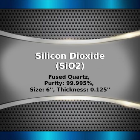
Silicon Dioxide (SiO2) Sputtering Targets, Fused Quartz, Purity: 99.995%, Size: 6”, Thickness: 0.125”

$269.00

Product 

Silicon Dioxide (SiO2) Sputtering Targets, Fused Quartz, Purity: 99.995%, Size: 6'', Thickness: 0.125''

CAS No.

7631-86-9

Appearance

Powder

Purity

≥99%,  ≥99.9%,  ≥95%

(Other purities are also available)

APS

N/A  (Size Can be customized), Ask for other available size ranges.

Ingredient

N/A

Molecular Weight

60.08 g/mol

Melting Point

~1710°C

Boiling Point

 ~2,950 °C

Density

~2.20 g/cm³

Product Codes

NCZ-1712K

Copper (Cu) Sputtering Targets, Purity: 99.999%, Size: 6”, Thickness: 0.250”

$270.00

Applications of Sputtering Targets;

Film deposition is accomplished using sputtering targets. A technique for sputtering thin films is called "deposition made by sputter targets," which entails eroding material from a "target" source onto a "substrate" like a silicon wafer. Etching of the target is done using semiconductor sputtering targets. When selectivity is not an issue and a high degree of etching anisotropy is required, sputter etching is the method of choice. By removing the target material through etching, sputter targets are also utilized for investigation. In secondary ion spectroscopy (SIMS), one example is when the target material is sputtered at a steady pace. Mass spectrometry is used to quantify the concentration and identity of spewed atoms as the target is sputtered.

The target material's composition may be ascertained and even very low concentrations of contaminants can be found with the aid of the sputtering target.

There is also an application area for sputtering targets in space. One type of space weathering that alters the chemical and physical characteristics of airless worlds like the Moon and asteroids is sputtering.

Aluminum (Al) Sputtering Targets, Purity: 99.999%, Size: 6”, Thickness: 0.250”

$270.00

Product 

Aluminum (Al) Sputtering Targets, Purity: 99.999%, Size: 6'', Thickness: 0.250''

CAS No.

 7429-90-5

Appearance

Powder

Purity

≥99%,  ≥99.9%,  ≥95%

(Other purities are also available)

APS

N/A (Size Can be customized), Ask for other available size ranges.

Ingredient

N/A

Molecular Weight

 26.98 g/mol

Melting Point

 660.3 °C

Boiling Point

 2519 °C

Density

 2.70 g/cm³

Product Codes

NCZ-2566K

Samarium (Sm) Sputtering Target

Price range: $272.00 through $803.00
Select options This product has multiple variants. The options may be chosen on the product page

Product 

Samarium (Sm) Sputtering Target

CAS No.

7440-19-9

Appearance

Powder

Purity

≥99%,  ≥99.9%,  ≥95%

(Other purities are also available)

APS

 NA (Size Can be customized), Ask for other available size ranges.

Ingredient

N/A

Molecular Weight

 150.36 g/mol

Melting Point

 1,072 °C

Boiling Point

 1,794 °C

Density

7.54 g/cm³

Product Codes

NCZ-1302K

Silicon Nitride (Si3N4) Sputtering Targets, Purity: 99.9%, Size: 1”, Thickness: 0.125”, White to Gray

$272.00

Product 

Silicon Nitride (Si3N4) Sputtering Targets, Purity: 99.9%, Size: 1'', Thickness: 0.125'', White to Gray

CAS No.

 12033-89-5

Appearance

Powder

Purity

≥99%,  ≥99.9%,  ≥95%

(Other purities are also available)

APS

N/A  (Size Can be customized), Ask for other available size ranges.

Ingredient

N/A

Molecular Weight

 140.28 g/mol

Melting Point

 ~1900 °C

Boiling Point

N/A

Density

~3.2 g/cm³

Product Codes

NCZ-1704K

Boron (B) Sputtering Targets, Purity: 99.9%, Size: 2”, Thickness: 0.125”

$273.00

Applications of Sputtering Targets;

Film deposition is accomplished using sputtering targets. A technique for sputtering thin films is called "deposition made by sputter targets," which entails eroding material from a "target" source onto a "substrate" like a silicon wafer. Etching of the target is done using semiconductor sputtering targets. When selectivity is not an issue and a high degree of etching anisotropy is required, sputter etching is the method of choice. By removing the target material through etching, sputter targets are also utilized for investigation. In secondary ion spectroscopy (SIMS), one example is when the target material is sputtered at a steady pace. Mass spectrometry is used to quantify the concentration and identity of spewed atoms as the target is sputtered.

The target material's composition may be ascertained and even very low concentrations of contaminants can be found with the aid of the sputtering target.

There is also an application area for sputtering targets in space. One type of space weathering that alters the chemical and physical characteristics of airless worlds like the Moon and asteroids is sputtering.

Boron (B) Sputtering Targets, Purity: 99.9%, Size: 2”, Thickness: 0.125”

$273.00

Applications of Sputtering Targets;

Film deposition is accomplished using sputtering targets. A technique for sputtering thin films is called "deposition made by sputter targets," which entails eroding material from a "target" source onto a "substrate" like a silicon wafer. Etching of the target is done using semiconductor sputtering targets. When selectivity is not an issue and a high degree of etching anisotropy is required, sputter etching is the method of choice. By removing the target material through etching, sputter targets are also utilized for investigation. In secondary ion spectroscopy (SIMS), one example is when the target material is sputtered at a steady pace. Mass spectrometry is used to quantify the concentration and identity of spewed atoms as the target is sputtered.

The target material's composition may be ascertained and even very low concentrations of contaminants can be found with the aid of the sputtering target.

There is also an application area for sputtering targets in space. One type of space weathering that alters the chemical and physical characteristics of airless worlds like the Moon and asteroids is sputtering.

Praseodymium (Pr) Sputtering Targets, Purity: 99.9%, Size: 4”, Thickness: 0.125”

$273.00

Applications of Sputtering Targets;

Film deposition is accomplished using sputtering targets. A technique for sputtering thin films is called "deposition made by sputter targets," which entails eroding material from a "target" source onto a "substrate" like a silicon wafer. Etching of the target is done using semiconductor sputtering targets. When selectivity is not an issue and a high degree of etching anisotropy is required, sputter etching is the method of choice. By removing the target material through etching, sputter targets are also utilized for investigation. In secondary ion spectroscopy (SIMS), one example is when the target material is sputtered at a steady pace. Mass spectrometry is used to quantify the concentration and identity of spewed atoms as the target is sputtered.

The target material's composition may be ascertained and even very low concentrations of contaminants can be found with the aid of the sputtering target.

There is also an application area for sputtering targets in space. One type of space weathering that alters the chemical and physical characteristics of airless worlds like the Moon and asteroids is sputtering.

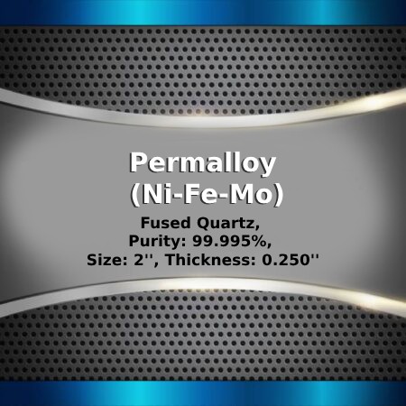
Permalloy (Ni-Fe-Mo) Sputtering Targets, Size: 2”, Thickness: 0.250”

$273.00

Product 

Permalloy (Ni-Fe-Mo) Sputtering Targets, Size: 2'', Thickness: 0.250''

CAS No.

 Nickel: 7440-02-0 Iron: 7439-89-6 Molybdenum: 7439-98-7

Appearance

Powder

Purity

≥99%,  ≥99.9%,  ≥95%

(Other purities are also available)

APS

N/A (Size Can be customized), Ask for other available size ranges.

Ingredient

N/A

Molecular Weight

 Not defined (alloy), but elemental weights: Ni: 58.69 g/mol Fe: 55.85 g/mol Mo: 95.95 g/mol

Melting Point

 ~1450 °C

Boiling Point

 ~2730–3000 °C

Density

~8.7 g/cm³

Product Codes

NCZ-1800K

Nickel (Ni) Sputtering Targets, Purity: 99.9%, Size: 4”, Thickness: 0.250”

$273.00

Product 

Nickel (Ni) Sputtering Targets, Purity: 99.9%, Size: 4'', Thickness: 0.250''

CAS No.

7440-02-0

Appearance

Powder

Purity

≥99%,  ≥99.9%,  ≥95%

(Other purities are also available)

APS

 N/A (Size Can be customized), Ask for other available size ranges.

Ingredient

N/A

Molecular Weight

 58.69 g/mol

Melting Point

 1,455 °C

Boiling Point

 2,732 °C

Density

 8.90 g/cm³

Product Codes

NCZ-1877K

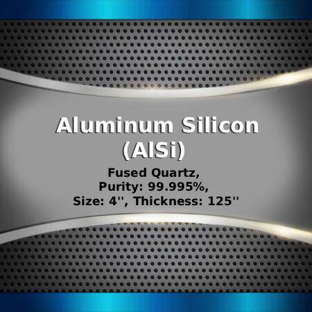
Aluminum Silicon (AlSi) Sputtering Targets, Purity: 99.999%, Size: 4”, Thickness: 0.125”

$273.00

Product 

Aluminum Silicon (AlSi) Sputtering Targets, Purity: 99.999%, Size: 4'', Thickness: 0.125''

CAS No.

Aluminum: 7429-90-5 Silicon: 7440-21-3

Appearance

Powder

Purity

≥99%,  ≥99.9%,  ≥95%

(Other purities are also available)

APS

N/A (Size Can be customized), Ask for other available size ranges.

Ingredient

N/A

Molecular Weight

 Al: 26.98 g/mol Si: 28.09 g/mol

Melting Point

 ~577–660 °C (depends on Si content)

Boiling Point

~2519 °C (approx.)

Density

~2.6–2.7 g/cm³

Product Codes

NCZ-2513K

Aluminum (Al) Sputtering Targets, Purity: 99.99%, Size: 6”, Thickness: 0.125”

$273.00

Product 

Aluminum (Al) Sputtering Targets, Purity: 99.99%, Size: 6'', Thickness: 0.125''

CAS No.

 7429-90-5

Appearance

Powder

Purity

≥99%,  ≥99.9%,  ≥95%

(Other purities are also available)

APS

N/A (Size Can be customized), Ask for other available size ranges.

Ingredient

N/A

Molecular Weight

 26.98 g/mol

Melting Point

 660.3 °C

Boiling Point

 2519 °C

Density

 2.70 g/cm³

Product Codes

NCZ-2569K

Aluminum (Al) Sputtering Targets, Purity: 99.999%, Size: 4”, Thickness: 0.250”

$273.00

Product 

Aluminum (Al) Sputtering Targets, Purity: 99.999%, Size: 4'', Thickness: 0.250''

CAS No.

 7429-90-5

Appearance

Powder

Purity

≥99%,  ≥99.9%,  ≥95%

(Other purities are also available)

APS

N/A (Size Can be customized), Ask for other available size ranges.

Ingredient

N/A

Molecular Weight

 26.98 g/mol

Melting Point

 660.3 °C

Boiling Point

 2519 °C

Density

 2.70 g/cm³

Product Codes

NCZ-2571K

Tantalum (Ta) Sputtering Targets, Purity: 99.95%, Size: 2”, Thickness: 0.125”

$274.00

Product 

Tantalum (Ta) Sputtering Targets, Purity: 99.95%, Size: 2'', Thickness: 0.125''

CAS No.

 7440-25-7

Appearance

Powder

Purity

≥99%,  ≥99.9%,  ≥95%

(Other purities are also available)

APS

N/A  (Size Can be customized), Ask for other available size ranges.

Ingredient

N/A

Molecular Weight

 180.95 g/mol

Melting Point

3017 °C

Boiling Point

 5458 °C

Density

16.65 g/cm³

Product Codes

NCZ-1665K

Magnesium (Mg) Sputtering Targets, Purity: 99.95%, Size: 4”, Thickness: 0.250”

$274.00

Product 

Magnesium (Mg) Sputtering Targets, Purity: 99.95%, Size: 4'', Thickness: 0.250''

CAS No.

7439-95-4

Appearance

Powder

Purity

≥99%,  ≥99.9%,  ≥95%

(Other purities are also available)

APS

 N/A (Size Can be customized), Ask for other available size ranges.

Ingredient

N/A

Molecular Weight

 24.305 g/mol

Melting Point

 650 °C

Boiling Point

 1,090 °C

Density

1.738 g/cm³

Product Codes

NCZ-1993K

Bismuth (Bi) Sputtering Targets, Purity: 99.999%, Size: 3”, Thickness: 0.125”

$275.00

Applications of Sputtering Targets;

Film deposition is accomplished using sputtering targets. A technique for sputtering thin films is called "deposition made by sputter targets," which entails eroding material from a "target" source onto a "substrate" like a silicon wafer.

Etching of the target is done using semiconductor sputtering targets. When selectivity is not an issue and a high degree of etching anisotropy is required, sputter etching is the method of choice. By removing the target material through etching, sputter targets are also utilized for investigation. In secondary ion spectroscopy (SIMS), one example is when the target material is sputtered at a steady pace. Mass spectrometry is used to quantify the concentration and identity of spewed atoms as the target is sputtered. With the sputtering target's assistance, the

There is also an application area for sputtering targets in space. One type of space weathering that alters the chemical and physical characteristics of airless worlds like the Moon and asteroids is sputtering.

The metal bismuth is silvery with a hint of pink and is fragile. Both in air and water, it is stable. Despite having poor thermal and electrical qualities, bismuth is used to create fusible alloys, a class of materials with low melting points that can be used in a variety of applications, such as thermal fuses and solders. Because pure bismuth exhibits a high absorption of gamma rays, it can be used as a window or filter for these particles while allowing neutrons to pass through.

Iron (Fe) Sputtering Targets, Purity: 99.99%, Size: 3”, Thickness: 0.125”

$275.00

Product 

Iron (Fe) Sputtering Targets, Purity: 99.99%, Size: 3'', Thickness: 0.125''

CAS No.
 7439-89-6

Appearance

Powder

Purity

≥99%,  ≥99.9%,  ≥95%

(Other purities are also available)

APS

 N/A (Size Can be customized), Ask for other available size ranges.

Ingredient

N/A

Molecular Weight

 55.85 g/mol

Melting Point

 1538 °C

Boiling Point

 2862 °C

Density

 7.87 g/cm³

Product Codes

NCZ-2181K

Bismuth (Bi) Sputtering Targets, Purity: 99.999%, Size: 1”, Thickness: 0.250”

$275.00

Product 

Bismuth (Bi) Sputtering Targets, Purity: 99.999%, Size: 1'', Thickness: 0.250''

CAS No.

7440‑69‑9

Appearance

Powder

Purity

≥99%,  ≥99.9%,  ≥95%

(Other purities are also available)

APS

1 – 5 µm (Size Can be customized), Ask for other available size ranges.

Ingredient

N/A

Molecular Weight

~208.98 g/mol

Melting Point

 271.4 °C

Boiling Point

~1560 °C

Density

 ~9.78–9.80 g/cm³

Product Codes

NCZ-2439K

Aluminum (Al) Sputtering Targets, Purity: 99.99%, Size: 8”, Thickness: 0.125”

$275.00

Product 

Aluminum (Al) Sputtering Targets, Purity: 99.99%, Size: 8'', Thickness: 0.125''

CAS No.

 7429-90-5

Appearance

Powder

Purity

≥99%,  ≥99.9%,  ≥95%

(Other purities are also available)

APS

N/A (Size Can be customized), Ask for other available size ranges.

Ingredient

N/A

Molecular Weight

 26.98 g/mol

Melting Point

 660.3 °C

Boiling Point

 2519 °C

Density

 2.70 g/cm³

Product Codes

NCZ-2565K

Magnesium (Mg) Sputtering Targets, Purity: 99.98%, Size: 5”, Thickness: 0.125”

$276.00

Applications of Sputtering Targets;

Film deposition is accomplished using sputtering targets. A technique for sputtering thin films is called "deposition made by sputter targets," which entails eroding material from a "target" source onto a "substrate" like a silicon wafer. Etching of the target is done using semiconductor sputtering targets. When selectivity is not an issue and a high degree of etching anisotropy is required, sputter etching is the method of choice. By removing the target material through etching, sputter targets are also utilized for investigation. In secondary ion spectroscopy (SIMS), one example is when the target material is sputtered at a steady pace. Mass spectrometry is used to quantify the concentration and identity of spewed atoms as the target is sputtered.

The target material's composition may be ascertained and even very low concentrations of contaminants can be found with the aid of the sputtering target.

There is also an application area for sputtering targets in space. One type of space weathering that alters the chemical and physical characteristics of airless worlds like the Moon and asteroids is sputtering.

Tungsten (W) Sputtering Targets, Purity: 99.95%, Size: 2”, Thickness: 0.250”

$276.00

Applications of Sputtering Targets;

Film deposition is accomplished using sputtering targets. A technique for sputtering thin films is called "deposition made by sputter targets," which entails eroding material from a "target" source onto a "substrate" like a silicon wafer. Etching of the target is done using semiconductor sputtering targets. When selectivity is not an issue and a high degree of etching anisotropy is required, sputter etching is the method of choice. By removing the target material through etching, sputter targets are also utilized for investigation. In secondary ion spectroscopy (SIMS), one example is when the target material is sputtered at a steady pace. Mass spectrometry is used to quantify the concentration and identity of spewed atoms as the target is sputtered.

The target material's composition may be ascertained and even very low concentrations of contaminants can be found with the aid of the sputtering target.

There is also an application area for sputtering targets in space. One type of space weathering that alters the chemical and physical characteristics of airless worlds like the Moon and asteroids is sputtering.

Zinc (Zn) Sputtering Targets, Purity: 99.95%, Size: 8”, Thickness: 0.250”

$276.00

Applications of Sputtering Targets;

Film deposition is accomplished using sputtering targets. A technique for sputtering thin films is called "deposition made by sputter targets," which entails eroding material from a "target" source onto a "substrate" like a silicon wafer. Etching of the target is done using semiconductor sputtering targets. When selectivity is not an issue and a high degree of etching anisotropy is required, sputter etching is the method of choice. By removing the target material through etching, sputter targets are also utilized for investigation. In secondary ion spectroscopy (SIMS), one example is when the target material is sputtered at a steady pace. Mass spectrometry is used to quantify the concentration and identity of spewed atoms as the target is sputtered.

The target material's composition may be ascertained and even very low concentrations of contaminants can be found with the aid of the sputtering target.

There is also an application area for sputtering targets in space. One type of space weathering that alters the chemical and physical characteristics of airless worlds like the Moon and asteroids is sputtering.

Titanium Dioxide (TiO2) Sputtering Targets, Purity: 99.9%, Size: 1”, Thickness: 0.125”, Grey to Black

$276.00

Product 

Titanium Dioxide (TiO2) Sputtering Targets, Purity: 99.9%, Size: 1'', Thickness: 0.125'', Grey to Black

CAS No.

13463‑67‑7

Appearance

Powder

Purity

≥99%,  ≥99.9%,  ≥95%

(Other purities are also available)

APS

TiO₂ (black granules) (Size Can be customized), Ask for other available size ranges.

Ingredient

N/A

Molecular Weight

79.94 g/mol

Melting Point

~1,843 °C

Boiling Point

~2,972 °C

Density

~4.23 g/cm³

Product Codes

NCZ-1445K

Yttrium (Y) Sputtering Targets, Purity: 99.9%, Size: 1”, Thickness: 0.250”

$277.00

Applications of Sputtering Targets;

  • Sputtering targets is used for film deposition. The deposition made by sputter targets is a method of depositing thin films by sputtering that involves eroding material from a "target" source onto a "substrate" such as  a silicon wafer.
  • Semiconductor sputtering targets is used to etch the target. Sputter etching is chosen in cases where a high degree of etching anisotropy is needed and selectivity is not a concern.
  • Sputter targets is also used for analysis by etching away the target material.
One of the example occurs in secondary ion spectroscopy (SIMS), where the target sample is sputtered at a constant rate. As the target is sputtered, the concentration and identity of sputtered atoms are measured using mass spectrometry. By helping of the sputtering target, the composition of the target material can be determined and even extremely low concentrations of impurities are detected. Sputtering target has also application area in space. Sputtering is one of the forms of space weathering, a process that changes the physical and chemical properties of airless bodies, such as asteroids and the Moon.

Nickel (Ni) Sputtering Targets, Purity: 99.995%, Size: 4”, Thickness: 0.125”

$277.00

Applications of Sputtering Targets;

Film deposition is accomplished using sputtering targets. A technique for sputtering thin films is called "deposition made by sputter targets," which entails eroding material from a "target" source onto a "substrate" like a silicon wafer. Etching of the target is done using semiconductor sputtering targets. When selectivity is not an issue and a high degree of etching anisotropy is required, sputter etching is the method of choice. By removing the target material through etching, sputter targets are also utilized for investigation. In secondary ion spectroscopy (SIMS), one example is when the target material is sputtered at a steady pace. Mass spectrometry is used to quantify the concentration and identity of spewed atoms as the target is sputtered.

By helping of the sputtering target, the composition of the target material may be evaluated and even extremely tiny amounts of contaminants are recognized.

There is also an application area for sputtering targets in space. One type of space weathering that alters the chemical and physical characteristics of airless worlds like the Moon and asteroids is sputtering.

Lithium Titanate (Li2TiO3) Sputtering Targets, indium, Purity: 99.95%, Size: 2”, Thickness: 0.125”

$280.00

Applications of Sputtering Targets;

Film deposition is accomplished using sputtering targets. A technique for sputtering thin films is called "deposition made by sputter targets," which entails eroding material from a "target" source onto a "substrate" like a silicon wafer. Etching of the target is done using semiconductor sputtering targets. When selectivity is not an issue and a high degree of etching anisotropy is required, sputter etching is the method of choice. By removing the target material through etching, sputter targets are also utilized for investigation. In secondary ion spectroscopy (SIMS), one example is when the target material is sputtered at a steady pace. Mass spectrometry is used to quantify the concentration and identity of spewed atoms as the target is sputtered.

By helping of the sputtering target, the composition of the target material may be evaluated and even extremely tiny amounts of contaminants are recognized.

There is also an application area for sputtering targets in space. One type of space weathering that alters the chemical and physical characteristics of airless worlds like the Moon and asteroids is sputtering.

Magnesium (Mg) Sputtering Targets, Purity: 99.98%, Size: 4”, Thickness: 0.250”

$280.00

Product 

Magnesium (Mg) Sputtering Targets, Purity: 99.98%, Size: 4'', Thickness: 0.250''

CAS No.

7439-95-4

Appearance

Powder

Purity

≥99%,  ≥99.9%,  ≥95%

(Other purities are also available)

APS

 N/A (Size Can be customized), Ask for other available size ranges.

Ingredient

N/A

Molecular Weight

 24.305 g/mol

Melting Point

 650 °C

Boiling Point

 1,090 °C

Density

1.738 g/cm³

Product Codes

NCZ-1992K

Nickel Vanadium (NiV) Sputtering Targets, Purity: 99.95%, Size: 2”, Thickness: 0.250”

$281.00

Product 

Nickel Vanadium (NiV) Sputtering Targets, Purity: 99.95%, Size: 2'', Thickness: 0.250''

CAS No.

11137-91-4

Appearance

Powder

Purity

≥99%,  ≥99.9%,  ≥95%

(Other purities are also available)

APS

N/A (Size Can be customized), Ask for other available size ranges.

Ingredient

N/A

Molecular Weight

~57.9 g/mol

Melting Point

~1,350–1,450 °C

Boiling Point

N/A

Density

 ~8.5 g/cm³

Product Codes

NCZ-1827K

Nickel Chromium (Ni-Cr) Sputtering Targets, Purity: 99.9%, Size: 3”, Thickness: 0.125”

$282.00

Applications of Sputtering Targets;

Film deposition is accomplished using sputtering targets. A technique for sputtering thin films is called "deposition made by sputter targets," which entails eroding material from a "target" source onto a "substrate" like a silicon wafer. Etching of the target is done using semiconductor sputtering targets. When selectivity is not an issue and a high degree of etching anisotropy is required, sputter etching is the method of choice. By removing the target material through etching, sputter targets are also utilized for investigation. In secondary ion spectroscopy (SIMS), one example is when the target material is sputtered at a steady pace. Mass spectrometry is used to quantify the concentration and identity of spewed atoms as the target is sputtered.

The target material's composition may be ascertained and even very low concentrations of contaminants can be found with the aid of the sputtering target.

There is also an application area for sputtering targets in space. One type of space weathering that alters the chemical and physical characteristics of airless worlds like the Moon and asteroids is sputtering.

Silicon Nitride (Si3N4) Sputtering Targets, Purity: 99.9%, Size: 1”, Thickness: 0.250”, White to Gray

$282.00

Applications of Sputtering Targets;

Film deposition is accomplished using sputtering targets. A technique for sputtering thin films is called "deposition made by sputter targets," which entails eroding material from a "target" source onto a "substrate" like a silicon wafer. Etching of the target is done using semiconductor sputtering targets. When selectivity is not an issue and a high degree of etching anisotropy is required, sputter etching is the method of choice. By removing the target material through etching, sputter targets are also utilized for investigation. In secondary ion spectroscopy (SIMS), one example is w

The target material's composition may be ascertained and even very low concentrations of contaminants can be found with the aid of the sputtering target.

There is also an application area for sputtering targets in space. One type of space weathering that alters the chemical and physical characteristics of airless worlds like the Moon and asteroids is sputtering.

hen the target material is sputtered at a steady pace. Mass spectrometry is used to quantify the concentration and identity of spewed atoms as the target is sputtered.

Titanium Dioxide (TiO2) Sputtering Targets, Purity: 99.9%, Size: 1”, Thickness: 0.250”, Grey to Black

$282.00

Applications of Sputtering Targets;

Film deposition is accomplished using sputtering targets. A technique for sputtering thin films is called "deposition made by sputter targets," which entails eroding material from a "target" source onto a "substrate" like a silicon wafer. Etching of the target is done using semiconductor sputtering targets. When selectivity is not an issue and a high degree of etching anisotropy is required, sputter etching is the method of choice. By removing the target material through etching, sputter targets are also utilized for investigation. In secondary ion spectroscopy (SIMS), one example is when the target material is sputtered at a steady pace. Mass spectrometry is used to quantify the concentration and identity of spewed atoms as the target is sputtered.

The target material's composition may be ascertained and even very low concentrations of contaminants can be found with the aid of the sputtering target.

There is also an application area for sputtering targets in space. One type of space weathering that alters the chemical and physical characteristics of airless worlds like the Moon and asteroids is sputtering.

Vanadium (V) Sputtering Targets, Purity: 99.5%, Size: 2”, Thickness: 0.250”

$282.00

Applications of Sputtering Targets;

Film deposition is accomplished using sputtering targets. A technique for sputtering thin films is called "deposition made by sputter targets," which entails eroding material from a "target" source onto a "substrate" like a silicon wafer. Etching of the target is done using semiconductor sputtering targets. When selectivity is not an issue and a high degree of etching anisotropy is required, sputter etching is the method of choice. By removing the target material through etching, sputter targets are also utilized for investigation. In secondary ion spectroscopy (SIMS), one example is when the target material is sputtered at a steady pace. Mass spectrometry is used to quantify the concentration and identity of spewed atoms as the target is sputtered.

Nickel (Ni) Sputtering Targets, Purity: 99.99%, Size: 4”, Thickness: 0.250”

$283.00

Product 

Nickel (Ni) Sputtering Targets, Purity: 99.99%, Size: 4'', Thickness: 0.250''

CAS No.

7440-02-0

Appearance

Powder

Purity

≥99%,  ≥99.9%,  ≥95%

(Other purities are also available)

APS

 N/A (Size Can be customized), Ask for other available size ranges.

Ingredient

N/A

Molecular Weight

 58.69 g/mol

Melting Point

 1,455 °C

Boiling Point

 2,732 °C

Density

 8.90 g/cm³

Product Codes

NCZ-1876K

Bismuth (Bi) Sputtering Target

Price range: $284.00 through $762.00
Select options This product has multiple variants. The options may be chosen on the product page

Product 

Bismuth (Bi) Sputtering Target

CAS No.

7440-69-9

Appearance

Powder

Purity

≥99%,  ≥99.9%,  ≥95%

(Other purities are also available)

APS

 NA (Size Can be customized), Ask for other available size ranges.

Ingredient

N/A

Molecular Weight

208.98 g/mol

Melting Point

271.4 °C

Boiling Point

 1,560 °C

Density

9.78 g/cm³

Product Codes

NCZ-1347K

Cerium (Ce) Sputtering Target

Price range: $284.00 through $762.00
Select options This product has multiple variants. The options may be chosen on the product page

Product 

Cerium (Ce) Sputtering Target

CAS No.

7440-45-1

Appearance

Powder

Purity

≥99%,  ≥99.9%,  ≥95%

(Other purities are also available)

APS

 NA (Size Can be customized), Ask for other available size ranges.

Ingredient

N/A

Molecular Weight

140.12 g/mol

Melting Point

798 °C

Boiling Point

3,426 °C

Density

6.77 g/cm³

Product Codes

NCZ-1350K

Erbium (Er) Sputtering Target

Price range: $284.00 through $762.00
Select options This product has multiple variants. The options may be chosen on the product page

Product 

Erbium (Er) Sputtering Target

CAS No.

 7429-91-6

Appearance

Powder

Purity

≥99%,  ≥99.9%,  ≥95%

(Other purities are also available)

APS

 NA (Size Can be customized), Ask for other available size ranges.

Ingredient

N/A

Molecular Weight

162.5 g/mol

Melting Point

1,407 °C

Boiling Point

2,567 °C

Density

8.55 g/cm³

Product Codes

NCZ-1354K

Strontium (Sr) Sputtering Target

Price range: $284.00 through $762.00
Select options This product has multiple variants. The options may be chosen on the product page

Product 

Strontium (Sr) Sputtering Target

CAS No.

7440-24-6

Appearance

Powder

Purity

≥99%,  ≥99.9%,  ≥95%

(Other purities are also available)

APS

 NA (Size Can be customized), Ask for other available size ranges.

Ingredient

N/A

Molecular Weight

87.62 g/mol

Melting Point

777 °C

Boiling Point

 1,382 °C

Density

 2.64 g/cm³

Product Codes

NCZ-1360K

Yttrium (Y) Sputtering Target

Price range: $284.00 through $762.00
Select options This product has multiple variants. The options may be chosen on the product page

Product 

Yttrium (Y) Sputtering Target

CAS No.

7440-65-5

Appearance

Powder

Purity

≥99%,  ≥99.9%,  ≥95%

(Other purities are also available)

APS

 NA (Size Can be customized), Ask for other available size ranges.

Ingredient

N/A

Molecular Weight

88.91 g/mol

Melting Point

 1,522 °C

Boiling Point

 3,345 °C

Density

 4.47 g/cm³

Product Codes

NCZ-1364K

Bismuth Oxide (Bi2O3) Sputtering Target

Price range: $284.00 through $762.00
Select options This product has multiple variants. The options may be chosen on the product page

Product 

Bismuth Oxide (Bi2O3) Sputtering Target

CAS No.

1304-76-3

Appearance

Powder

Purity

≥99%,  ≥99.9%,  ≥95%

(Other purities are also available)

APS

 NA (Size Can be customized), Ask for other available size ranges.

Ingredient

N/A

Molecular Weight

465.96 g/mol

Melting Point

 817 °C

Boiling Point

~1,890 °C

Density

 8.9 – 9.3 g/cm³

Product Codes

NCZ-1366K

Chromium Oxide (Cr2O3) Sputtering Target

Price range: $284.00 through $762.00
Select options This product has multiple variants. The options may be chosen on the product page

Product 

Chromium Oxide (Cr2O3) Sputtering Target

CAS No.

 1308-38-9

Appearance

Powder

Purity

≥99%,  ≥99.9%,  ≥95%

(Other purities are also available)

APS

 NA (Size Can be customized), Ask for other available size ranges.

Ingredient

N/A

Molecular Weight

151.99 g/mol

Melting Point

2,435 °C

Boiling Point

N/A

Density

5.22 g/cm³

Product Codes

NCZ-1367K

Cobalt Oxide (CoO) Sputtering Target

Price range: $284.00 through $762.00
Select options This product has multiple variants. The options may be chosen on the product page

Product 

Cobalt Oxide (CoO) Sputtering Target

CAS No.

1307-96-6

Appearance

Powder

Purity

≥99%,  ≥99.9%,  ≥95%

(Other purities are also available)

APS

 NA (Size Can be customized), Ask for other available size ranges.

Ingredient

N/A

Molecular Weight

74.93 g/mol

Melting Point

1,935 °C

Boiling Point

Decomposes (~2,000 °C+)

Density

 6.45 g/cm³

Product Codes

NCZ-1368K

Lanthanum Oxide (La2O3) Sputtering Target

Price range: $284.00 through $762.00
Select options This product has multiple variants. The options may be chosen on the product page

Product 

Lanthanum Oxide (La2O3) Sputtering Target

CAS No.

1312-81-8

Appearance

Powder

Purity

≥99%,  ≥99.9%,  ≥95%

(Other purities are also available)

APS

 NA (Size Can be customized), Ask for other available size ranges.

Ingredient

N/A

Molecular Weight

 325.81 g/mol

Melting Point

2,313 °C

Boiling Point

~4,200 °C

Density

6.51 g/cm³

Product Codes

NCZ-1372K

Samarium Oxide (Sm2O3) Sputtering Target

Price range: $284.00 through $762.00
Select options This product has multiple variants. The options may be chosen on the product page

Product 

Samarium Oxide (Sm2O3) Sputtering Target

CAS No.

 12060‑58‑1

Appearance

Powder

Purity

≥99%,  ≥99.9%,  ≥95%

(Other purities are also available)

APS

 NA (Size Can be customized), Ask for other available size ranges.

Ingredient

N/A

Molecular Weight

~348.8 g/mol

Melting Point

~2,335 °C

Boiling Point

~4,118 °C

Density

 ~8.35 – 7.60 g/cm³

Product Codes

NCZ-1376K

Silicon Nitride (Si3N4) Sputtering Target

Price range: $284.00 through $762.00
Select options This product has multiple variants. The options may be chosen on the product page

Product 

Silicon Nitride (Si3N4) Sputtering Target

CAS No.

12033‑89‑5

Appearance

Powder

Purity

≥99%,  ≥99.9%,  ≥95%

(Other purities are also available)

APS

 NA (Size Can be customized), Ask for other available size ranges.

Ingredient

N/A

Molecular Weight

 140.28 g/mol

Melting Point

~1,900 °C

Boiling Point

N/A

Density

 ~2.2–3.5 g/cm³

Product Codes

NCZ-1382K

Silicon (Si) Sputtering Targets, N-type, Purity: 99.999%, Size: 1”, Thickness: 0.250”

$284.00

Product 

Silicon (Si) Sputtering Targets, N-type, Purity: 99.999%, Size: 1'', Thickness: 0.250''

CAS No.

7440-21-3

Appearance

Powder

Purity

≥99%,  ≥99.9%,  ≥95%

(Other purities are also available)

APS

N/A  (Size Can be customized), Ask for other available size ranges.

Ingredient

N/A

Molecular Weight

28.0855 g/mol

Melting Point

 1,414 °C

Boiling Point

3,265 °C

Density

 2.33 g/cm³

Product Codes

NCZ-1766K

Calcium Manganate (CaMnO3) Sputtering Targets, Purity: 99.9%, Size: 1”, Thickness: 0.125”

$285.00

Applications of Sputtering Targets;

Film deposition is accomplished using sputtering targets. A technique for sputtering thin films is called "deposition made by sputter targets," which entails eroding material from a "target" source onto a "substrate" like a silicon wafer. Etching of the target is done using semiconductor sputtering targets. When selectivity is not an issue and a high degree of etching anisotropy is required, sputter etching is the method of choice. By removing the target material through etching, sputter targets are also utilized for investigation. In secondary ion spectroscopy (SIMS), one example is when the target material is sputtered at a steady pace. Mass spectrometry is used to quantify the concentration and identity of spewed atoms as the target is sputtered.

The target material's composition may be ascertained and even very low concentrations of contaminants can be found with the aid of the sputtering target.

There is also an application area for sputtering targets in space. One type of space weathering that alters the chemical and physical characteristics of airless worlds like the Moon and asteroids is sputtering.

Copper (Cu) Sputtering Targets, Purity: 99.999%, Size: 4”, Thickness: 0.125”

$285.00

Applications of Sputtering Targets;

Film deposition is accomplished using sputtering targets. A technique for sputtering thin films is called "deposition made by sputter targets," which entails eroding material from a "target" source onto a "substrate" like a silicon wafer. Etching of the target is done using semiconductor sputtering targets. When selectivity is not an issue and a high degree of etching anisotropy is required, sputter etching is the method of choice. By removing the target material through etching, sputter targets are also utilized for investigation. In secondary ion spectroscopy (SIMS), one example is when the target material is sputtered at a steady pace. Mass spectrometry is used to quantify the concentration and identity of spewed atoms as the target is sputtered.

The target material's composition may be ascertained and even very low concentrations of contaminants can be found with the aid of the sputtering target.

There is also an application area for sputtering targets in space. One type of space weathering that alters the chemical and physical characteristics of airless worlds like the Moon and asteroids is sputtering.

Bismuth (Bi) Sputtering Targets, Purity: 99.999%, Size: 3”, Thickness: 0.250”

$286.00

Applications of Sputtering Targets;

Film deposition is accomplished using sputtering targets. A technique for sputtering thin films is called "deposition made by sputter targets," which entails eroding material from a "target" source onto a "substrate" like a silicon wafer. Etching of the target is done using semiconductor sputtering targets. When selectivity is not an issue and a high degree of etching anisotropy is required, sputter etching is the method of choice. By removing the target material through etching, sputter targets are also utilized for investigation. In secondary ion spectroscopy (SIMS), one example is when the target material is sputtered at a steady pace. Mass spectrometry is used to quantify the concentration and identity of spewed atoms as the target is sputtered. With the sputtering target's assistance, the

Applications for sputtering targets are also found in space. Sputtering is a type of space weathering, a process that modifies the chemical and physical characteristics of asteroids and the Moon, among other airless planets.

The silvery metal bismuth has a hint of pink and is fragile. It is stable in both water and air. Even though bismuth has bad thermal and electrical properties, it is used to make fusible alloys, a class of materials with low melting points that are useful for a variety of products, such as thermal fuses and solders. While allowing neutrons to flow through, pure bismuth exhibits a strong absorption of gamma rays, making it suitable as a filter or window for these particles.

Nickel Vanadium (NiV) Sputtering Targets, Purity: 99.95%, Size: 3”, Thickness: 0.250”

$286.00

Applications of Sputtering Targets;

Film deposition is accomplished using sputtering targets. A technique for sputtering thin films is called "deposition made by sputter targets," which entails eroding material from a "target" source onto a "substrate" like a silicon wafer. Etching of the target is done using semiconductor sputtering targets. When selectivity is not an issue and a high degree of etching anisotropy is required, sputter etching is the method of choice. By removing the target material through etching, sputter targets are also utilized for investigation. In secondary ion spectroscopy (SIMS), one example is when the target material is sputtered at a steady pace. Mass spectrometry is used to quantify the concentration and identity of spewed atoms as the target is sputtered.

The target material's composition may be ascertained and even very low concentrations of contaminants can be found with the aid of the sputtering target.

There is also an application area for sputtering targets in space. One type of space weathering that alters the chemical and physical characteristics of airless worlds like the Moon and asteroids is sputtering.

Silicon (Si) Sputtering Targets, N-type, Purity: 99.999%, Size: 2”, Thickness: 0.250”

$286.00

Applications of Sputtering Targets;

Film deposition is accomplished using sputtering targets. A technique for sputtering thin films is called "deposition made by sputter targets," which entails eroding material from a "target" source onto a "substrate" like a silicon wafer. Etching of the target is done using semiconductor sputtering targets. When selectivity is not an issue and a high degree of etching anisotropy is required, sputter etching is the method of choice. By removing the target material through etching, sputter targets are also utilized for investigation. In secondary ion spectroscopy (SIMS), one example is when the target material is sputtered at a steady pace. Mass spectrometry is used to quantify the concentration and identity of spewed atoms as the target is sputtered.

The target material's composition may be ascertained and even very low concentrations of contaminants can be found with the aid of the sputtering target.

There is also an application area for sputtering targets in space. One type of space weathering that alters the chemical and physical characteristics of airless worlds like the Moon and asteroids is sputtering.

Molybdenum (Mo) Sputtering Targets, Purity: 99.95%, Size: 8”, Thickness: 0.250”

$288.00

Applications of Sputtering Targets;

For film deposition, sputtering targets are employed. A sputtering technique called "deposition made by sputter targets" entails eroding material from a "target" source onto a "substrate" like a silicon wafer. Targets are etched using semiconductor sputtering targets. When etching anisotropy is required to a great degree and selectivity is not an issue, sputter etching is the method of choice. By etching away the target material, sputter targets are also utilized for investigation. In one instance, the target sample is sputtered at a steady pace in secondary ion spectroscopy (SIMS). Using mass spectrometry, the concentration and identity of the spewed atoms are determined when the target is sputtered.

By helping of the sputtering target, the composition of the target material may be evaluated and even extremely tiny amounts of contaminants are recognized.

There is also an application area for sputtering targets in space. One type of space weathering that alters the chemical and physical characteristics of airless worlds like the Moon and asteroids is sputtering.

Selenium (Se) Sputtering Targets, Purity: 99.999%, Size: 3”, Thickness: 0.125”

$288.00

Applications of Sputtering Targets;

Film deposition is accomplished using sputtering targets. A technique for sputtering thin films is called "deposition made by sputter targets," which entails eroding material from a "target" source onto a "substrate" like a silicon wafer. Etching of the target is done using semiconductor sputtering targets. When selectivity is not an issue and a high degree of etching anisotropy is required, sputter etching is the method of choice. By removing the target material through etching, sputter targets are also utilized for investigation. In secondary ion spectroscopy (SIMS), one example is when the target material is sputtered at a steady pace. Mass spectrometry is used to quantify the concentration and identity of spewed atoms as the target is sputtered.

The target material's composition may be ascertained and even very low concentrations of contaminants can be found with the aid of the sputtering target.

There is also an application area for sputtering targets in space. One type of space weathering that alters the chemical and physical characteristics of airless worlds like the Moon and asteroids is sputtering.

Boron Nitride (BN) Sputtering Target

Price range: $288.00 through $852.00
Select options This product has multiple variants. The options may be chosen on the product page

Product 

Boron Nitride (BN) Sputtering Target

CAS No.

10043-11-5

Appearance

Powder

Purity

≥99%,  ≥99.9%,  ≥95%

(Other purities are also available)

APS

 NA (Size Can be customized), Ask for other available size ranges.

Ingredient

N/A

Molecular Weight

24.82 g/mol

Melting Point

~2,973 °C

Boiling Point

N/A

Density

 ~2.1–3.5 g/cm³

Product Codes

NCZ-1333K