• CONTACT US
  • FAQs
FREE SHIPPING WITHIN CANADA FOR ALL ORDER OF 300$
0 Compare
0 Wishlist
Login / Register
  • Home
  • Products
  • Contact Us
Menu
1 item / $788.00
Browse Categories
  • 3D Printer Materials
  • BATTERY EQUIPMENT
  • CARBON NANOTUBES
  • DISPERSIONS
  • MICROPARTICLES
  • MXene and MAXene
  • NANOPARTICLES & NANOPOWDERS
  • RARE EARTH MATERIALS
  • SILICON WAFERS & SEMICONDUCTOR WAFERS
24/7 SUPPORT

+1-780-612-4177

1 item / $788.00
View cart “Yttrium Ferrite (Y3Fe5O12) Sputtering Targets, Purity: 99.9%, Size: 1”, Thickness: 0.250”” has been added to your cart.
Click to enlarge
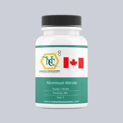
HomeSputtering TargetsSputtering Targets Names A - CAluminum Nitride Sputtering Targets3" Aluminum Nitride (AlN) Sputtering Targets, Purity: 99.8%, Size: 3”, Thickness: 0.125”
Previous product
Aluminum Nitride (AlN) Sputtering Targets, Purity: 99.8%, Size: 3'', Thickness: 0.250'' $983.00
Back to products
Next product
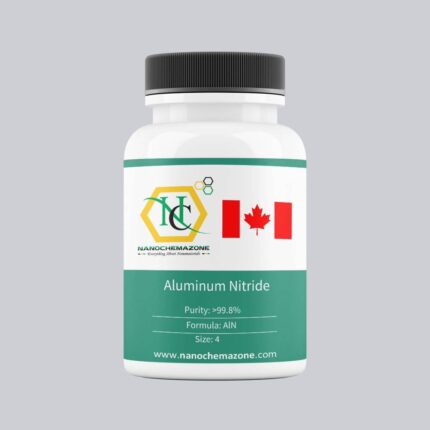
Aluminum Nitride (AlN) Sputtering Targets, Purity: 99.8%, Size:4'', Thickness: 0.250'' $1,213.00

Aluminum Nitride (AlN) Sputtering Targets, Purity: 99.8%, Size: 3”, Thickness: 0.125”

$744.00

Applications of Sputtering Targets;

  • Sputtering targets is used for film deposition. The deposition made by sputter targets is a method of depositing thin films by sputtering
    that involves eroding material from a “target” source onto a “substrate” such as  a silicon wafer.
  • Semiconductor sputtering targets is used to etch the target. Sputter etching is chosen in cases where a high degree of etching anisotropy
    is needed and selectivity is not a concern.
  • Sputter targets is also used for analysis by etching away the target material.

One of the example occurs in secondary ion spectroscopy (SIMS), where the target sample is sputtered at a constant rate. As the target is sputtered,
the concentration and identity of sputtered atoms are measured using mass spectrometry. By helping of the sputtering target, the composition of the
target material can be determined and even extremely low concentrations of impurities are detected.

Sputtering target has also application area in space. Sputtering is one of the forms of space weathering, a process that changes the physical and
chemical properties of airless bodies, such as asteroids and the Moon.

Aluminum nitride is a chemical compound with the formula of AlN.Aluminum nitride has excellent combination of physical, chemical, and mechanical
properties. High-quality films of aluminum nitride have been used in various devices and sensors including the optical and optoelectronic devices. As
far as the optical and optoelectronic applications are concerned, wide band gap (~6.2 eV) along with high-refractive index (~2.0) and low-absorption
coefficient (<10−3) makes AlN a very attractive material for these applications. In addition to this, thermal and chemical stability of AlN films make it
suitable for applications in difficult environment.

Today, AlN films/coatings have been grown by several methods which include pulsed laser deposition, reactive molecular beam epitaxy, vacuum
arc/cathodic arc deposition, DC/RF reactive sputtering, ion beam sputtering, metal-organic chemical vapor deposition (MOCVD), and miscellaneous
other techniques. Due to simplicity, reproducibility, ease of scaling up, and lower cost, magnetron sputtering is one of the common methods for growing
AlN films for various applications.

Properties of AlN films depend upon the crystal structure, crystal orientation, microstructure, and chemical composition, which in turn depend upon
the deposition conditions such as sputtering power, pulse frequency, duty cycle, growth temperature, nitrogen/argon flow ratio, and sputtering gas
pressure. AlN sputtering targets give good result with the method of reactive DC magnetron sputtering system.

Compare
Add to wishlist
Categories: 3", Aluminum Nitride Sputtering Targets, Sputtering Targets, Sputtering Targets Names A - C
Share
  • Description
  • Shipping & Delivery
Description

Aluminum Nitride (AlN) Sputtering Targets

Purity: 99.8%, Size: 3”, Thickness: 0.125”  

Sputtering is a proven technology capable of depositing thin films from a wide variety of materials on to diverse substrate shapes and sizes.
The process with sputter targets is repeatable and can be scaled up from small research and development projects. The proses with sputter
targets can be adapted to the production batches involving medium to large substrate areas. The chemical reaction can occur on the target
surface, in-flight or on the substrate depending on the process parameters. The many parameters make sputter deposition a complex process
but allow experts a large degree of control over the growth and microstructure of the area.

Shipping & Delivery

Related products

Erbium Oxide (Er2O3) Sputtering Targets, Purity: 99.99%, Size: 3”, Thickness: 0.250”

SPUTTERING TARGETS NAMES D - M, Erbium Oxide Sputtering Targets, Rare Earth Materials, Rare Earth Sputtering Targets, Sputtering Targets
$186.00
Select options
Compare
Quick view
Add to wishlist
Close

Ytterbium Oxide (Yb2O3) Sputtering Targets, Purity: 99.99%, Size: 3”, Thickness: 0.125”

YTTERBIUM OXIDE SPUTTERING TARGETS, 3, Rare Earth Sputtering Targets, Sputtering Targets, SPUTTERING TARGETS NAMES T - Z
$575.00
Add to cart
Compare
Quick view
Add to wishlist
Close

Erbium Oxide (Er2O3) Sputtering Targets, Purity: 99.99%, Size: 2”, Thickness:0.125”

SPUTTERING TARGETS NAMES D - M, Erbium Oxide Sputtering Targets, Rare Earth Materials, Rare Earth Sputtering Targets, Sputtering Targets
$138.00
Select options
Compare
Quick view
Add to wishlist
Close

Yttrium Ferrite (Y3Fe5O12) Sputtering Targets, Purity: 99.9%, Size: 1”, Thickness: 0.250”

YTTRIUM FERRITE SPUTTERING TARGETS, 1, Sputtering Targets, SPUTTERING TARGETS NAMES T - Z
$788.00
Add to cart
Compare
Quick view
Add to wishlist
Close

Yttrium (Y) Sputtering Targets, Purity: 99.9%, Size: 2”, Thickness: 0.250”

YTTRIUM SPUTTERING TARGETS, 2, Sputtering Targets, SPUTTERING TARGETS NAMES T - Z
$464.00
Add to cart
Compare
Quick view
Add to wishlist
Close

Yttrium (Y) Sputtering Targets, Purity: 99.9%, Size: 4”, Thickness: 0.250”

YTTRIUM SPUTTERING TARGETS, 4, Sputtering Targets, SPUTTERING TARGETS NAMES T - Z
$767.00
Add to cart
Compare
Quick view
Add to wishlist
Close

Ytterbium Oxide (Yb2O3) Sputtering Targets, indium, Purity: 99.9%, Size: 2”, Thickness: 0.125”

YTTERBIUM OXIDE SPUTTERING TARGETS, 2, Sputtering Targets, SPUTTERING TARGETS NAMES T - Z
$580.00
Add to cart
Compare
Quick view
Add to wishlist
Close

Erbium Oxide (Er2O3) Sputtering Targets, Purity: 99.99%, Size: 1”, Thickness: 0.250”

SPUTTERING TARGETS NAMES D - M, Erbium Oxide Sputtering Targets, Rare Earth Materials, Rare Earth Sputtering Targets, Sputtering Targets
$214.00
Select options
Compare
Quick view
Add to wishlist
Close

FREE SHIPPING

Carrier information.

ONLINE PAYMENT

Payment methods.

24/7 SUPPORT

Unlimited help desk.

100% SAFE

View our benefits.

FREE RETURNS

Track or cancel orders.

  • QUICK LINKS
    • About Us
    • Catalogue
    • Quotation
    • FAQ's
    • Products

  • CATEGORIES
    • MXene and MAXene
    • Wafers
    • Nanoparticles
    • Advanced Nanomaterials
    • Artificial Biological Solutions

  • POLICIES
    • Privacy Policy
    • Returns
    • Terms &amp; Conditions
    • Contact Us
    • Our Sitemap

AVAILABLE ON:

Payment System:
payment
Shipping System:
shipping

©NANOCHEMAZONE @ 2015-24 | All Rights Reserved
  • Menu
  • Categories
  • 3D Printer Materials
  • BATTERY EQUIPMENT
  • CARBON NANOTUBES
  • DISPERSIONS
  • MICROPARTICLES
  • MXene and MAXene
  • NANOPARTICLES & NANOPOWDERS
  • RARE EARTH MATERIALS
  • SILICON WAFERS & SEMICONDUCTOR WAFERS
  • Home
  • Shop
  • Blog
  • About us
  • Wishlist
  • Compare
  • Login / Register
Shopping cart
close

Sign in

close

Lost your password?

No account yet?

Create an Account
Shop
0 Wishlist
1 item Cart
My account